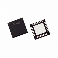
C8051F321-GM Silicon Laboratories Inc, C8051F321-GM Datasheet - Page 248

C8051F321-GM
Manufacturer Part Number
C8051F321-GM
Description
IC 8051 MCU 16K FLASH 28MLP
Manufacturer
Silicon Laboratories Inc
Series
C8051F32xr
Datasheets
1.C8051F320-TB.pdf
(250 pages)
2.C8051F321-GMR.pdf
(2 pages)
3.C8051F321-GM.pdf
(256 pages)
Specifications of C8051F321-GM
Program Memory Type
FLASH
Program Memory Size
16KB (16K x 8)
Package / Case
28-VQFN Exposed Pad, 28-HVQFN, 28-SQFN, 28-DHVQFN
Core Processor
8051
Core Size
8-Bit
Speed
25MHz
Connectivity
SMBus (2-Wire/I²C), SPI, UART/USART, USB
Peripherals
Brown-out Detect/Reset, POR, PWM, Temp Sensor, WDT
Number Of I /o
21
Ram Size
2.25K x 8
Voltage - Supply (vcc/vdd)
2.7 V ~ 3.6 V
Data Converters
A/D 13x10b
Oscillator Type
Internal
Operating Temperature
-40°C ~ 85°C
Processor Series
C8051F3x
Core
8051
Data Bus Width
8 bit
Data Ram Size
2.25 KB
Interface Type
I2C/SMBus/SPI/UART/USB
Maximum Clock Frequency
25 MHz
Number Of Programmable I/os
21
Number Of Timers
4
Operating Supply Voltage
2.7 V to 3.6 V
Maximum Operating Temperature
+ 85 C
Mounting Style
SMD/SMT
3rd Party Development Tools
PK51, CA51, A51, ULINK2
Development Tools By Supplier
C8051F320DK
Minimum Operating Temperature
- 40 C
On-chip Adc
13-ch x 10-bit or 17-ch x 10-bit
No. Of I/o's
21
Ram Memory Size
1280Byte
Cpu Speed
25MHz
No. Of Timers
4
Rohs Compliant
Yes
Lead Free Status / RoHS Status
Lead free / RoHS Compliant
For Use With
336-1480 - DAUGHTER CARD TOOLSTCK C8051F321770-1006 - ISP 4PORT FOR SILABS C8051F MCU336-1449 - ADAPTER PROGRAM TOOLSTICK F321336-1260 - DEV KIT FOR C8051F320/F321
Eeprom Size
-
Lead Free Status / Rohs Status
Lead free / RoHS Compliant
Other names
336-1261
Available stocks
Company
Part Number
Manufacturer
Quantity
Price
Company:
Part Number:
C8051F321-GM
Manufacturer:
SiliconL
Quantity:
4 364
Part Number:
C8051F321-GM
Manufacturer:
SILICON LABS/芯科
Quantity:
20 000
Part Number:
C8051F321-GMR
Manufacturer:
SILICON LABS/芯科
Quantity:
20 000
C8051F320/1
D
Revision 1.1 to Revision 1.2
•
•
•
•
•
•
•
•
•
•
•
•
•
•
•
•
•
•
•
•
•
•
•
Revision 1.2 to Revision 1.3
•
•
•
Revision 1.3 to Revision 1.4
•
•
•
•
248
OCUMENT
Updated document with RoHS compliant information.
Updated Table 3.1, “Global Electrical Characteristics,” on page 28.
Updated package drawings in Section “4. Pinout and Package Definitions” on page 30.
Updated Figure “5.4 10-Bit ADC Track and Conversion Example Timing” on page 44. ADC takes 14
SAR clocks to convert a sample.
Added Max and Min values for Offset and Full Scale Error in Table 5.1, “ADC0 Electrical Characteris-
tics,” on page 54.
Updated Bias Generator specifications in Table 6.1, “Voltage Reference Electrical Characteristics,” on
page 56.
Added Max values for Comparator supply current in Table 7.1, “Comparator Electrical Characteristics,”
on page 66.
Updated Section “8. Voltage Regulator (REG0)” with decoupling and bypass capacitor requirements.
Updated Table 8.1, “Voltage Regulator Electrical Specifications,” on page 68.
Updated how to clear the EA bit in Section “9.3. Interrupt Handler”.
Added Table 11.2, “Flash Security Summary,” on page 109.
Added Section “11.4. Flash Write and Erase Guidelines” on page 110.
Updated Internal Oscillator Suspend Mode behavior in Section “13.1.2. Internal Oscillator Suspend
Mode”.
Updated OSCICN reset value in SFR Definition 13.1. “OSCICN: Internal Oscillator Control” on
page 118.
Corrected maximum SMBus transfer speed in Section “16. SMBus”.
Updated Table 16.4, “SMBus Status Decoding,” on page 184.
- Slave Transmitter (0101 0XX)
- Slave Receiver (0001 00X)
Replaced Tables 17.1 though 17.6 with a single table (Table 17.1, “Timer Settings for Standard Baud
Rates Using The Internal Oscillator,” on page 194).
Updated WCOL bit description in SFR Definition 18.2. “SPI0CN: SPI0 Control” on page 204.
Updated references to IT01CF in SFR Definition 19.1. TCON: Timer Control and SFR
Definition 19.2. TMOD: Timer Mode.
Added Step 7 to Watchdog Timer Usage in Section “20.3.2. Watchdog Timer Usage”.
Changed sample system clock frequencies in Table 20.3, “Watchdog Timer Timeout Intervals
page 239.
Removed references to boundary scan in Section “21. C2 Interface”.
Various formatting fixes.
Removed references to "Boundary Scan" in the C2 chapter.
Updated package drawings to reflect JEDEC-standard nomenclature and supplier variations.
Relaxed maximum VBUS Detection Input Threshold specification in Table 5.1 from 4.0 to 2.9 V.
Updated Table 8.1 on page 68.
Updated Table 15.2 on page 144.
Removed USB Register Definition INMAX.
Removed USB Register Definition OUTMAX.
C
HANGE
L
IST
Rev. 1.4
1
,” on


