MC908JB8ADWE Freescale Semiconductor, MC908JB8ADWE Datasheet - Page 136
MC908JB8ADWE
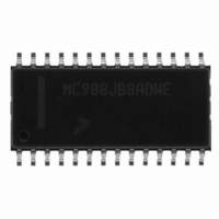
Manufacturer Part Number
MC908JB8ADWE
Description
IC MCU 3MHZ 8K FLASH 28-SOIC
Manufacturer
Freescale Semiconductor
Series
HC08r
Datasheet
1.MC908JB8JDWE.pdf
(286 pages)
Specifications of MC908JB8ADWE
Core Processor
HC08
Core Size
8-Bit
Speed
3MHz
Connectivity
USB
Peripherals
LVD, POR, PWM
Number Of I /o
21
Program Memory Size
8KB (8K x 8)
Program Memory Type
FLASH
Ram Size
256 x 8
Voltage - Supply (vcc/vdd)
4 V ~ 5.5 V
Oscillator Type
Internal
Operating Temperature
0°C ~ 70°C
Package / Case
28-SOIC (7.5mm Width)
Processor Series
HC08JB
Core
HC08
Data Bus Width
8 bit
Data Ram Size
256 B
Interface Type
USB
Maximum Clock Frequency
3 MHz
Number Of Programmable I/os
37
Number Of Timers
2
Operating Supply Voltage
5.25 V
Maximum Operating Temperature
+ 70 C
Mounting Style
SMD/SMT
Development Tools By Supplier
FSICEBASE, DEMO908GZ60E, M68EML08GZE, KITUSBSPIDGLEVME, KITUSBSPIEVME, KIT33810EKEVME
Minimum Operating Temperature
0 C
Controller Family/series
HC08
No. Of I/o's
21
Ram Memory Size
256Byte
Cpu Speed
8MHz
No. Of Timers
1
Embedded Interface Type
SCI, SPI
Rohs Compliant
Yes
Lead Free Status / RoHS Status
Lead free / RoHS Compliant
Eeprom Size
-
Data Converters
-
Lead Free Status / Rohs Status
Lead free / RoHS Compliant
Available stocks
Company
Part Number
Manufacturer
Quantity
Price

Part Number:
MC908JB8ADWE
Manufacturer:
FREESCALE
Quantity:
20 000


Universal Serial Bus Module (USB)
9.7.2.5 Data Signal Rise and Fall Time
Technical Data
136
For low-speed transmissions, the jitter time for any consecutive
differential data transitions must be within
any set of paired differential data transitions. These jitter numbers
include timing variations due to differential buffer delay, rise/fall time
mismatches, internal clock source jitter, noise and other random effects.
The output rise time and fall time are measured between 10% and 90%
of the signal. Edge transition time for the rising and falling edges of
low-speed signals is 75ns (minimum) into a capacitive load (C
200pF and 300ns (maximum) into a capacitive load of 600pF. The rising
and falling edges should be transitioning (monotonic) smoothly when
driving the cable to avoid excessive EMI.
DIFFERENTIAL
DATA LINES
t
Period
JITTER
Universal Serial Bus Module (USB)
Figure 9-14. Data Signal Rise and Fall Time
+
+
C
C
L
L
MC68HC908JB8•MC68HC08JB8•MC68HC08JT8 — Rev. 2.3
DIFFERENTIAL
DATA LINES
CONSECUTIVE
TRANSITIONS
Figure 9-13. Data Jitter
LOW SPEED: 75ns at C
10%
TRANSITIONS
RISE TIME
PAIRED
t
R
±
CROSSOVER
90%
25ns and within
POINTS
L
= 200pF, 300ns at C
Freescale Semiconductor
90%
FALL TIME
t
L
F
= 600 pF
10%
±
10ns for
L
) of
Related parts for MC908JB8ADWE
Image
Part Number
Description
Manufacturer
Datasheet
Request
R

Part Number:
Description:
Manufacturer:
Freescale Semiconductor, Inc
Datasheet:
Part Number:
Description:
Manufacturer:
Freescale Semiconductor, Inc
Datasheet:
Part Number:
Description:
Manufacturer:
Freescale Semiconductor, Inc
Datasheet:
Part Number:
Description:
Manufacturer:
Freescale Semiconductor, Inc
Datasheet:
Part Number:
Description:
Manufacturer:
Freescale Semiconductor, Inc
Datasheet:
Part Number:
Description:
Manufacturer:
Freescale Semiconductor, Inc
Datasheet:
Part Number:
Description:
Manufacturer:
Freescale Semiconductor, Inc
Datasheet:
Part Number:
Description:
Manufacturer:
Freescale Semiconductor, Inc
Datasheet:
Part Number:
Description:
Manufacturer:
Freescale Semiconductor, Inc
Datasheet:
Part Number:
Description:
Manufacturer:
Freescale Semiconductor, Inc
Datasheet:
Part Number:
Description:
Manufacturer:
Freescale Semiconductor, Inc
Datasheet:
Part Number:
Description:
Manufacturer:
Freescale Semiconductor, Inc
Datasheet:
Part Number:
Description:
Manufacturer:
Freescale Semiconductor, Inc
Datasheet:
Part Number:
Description:
Manufacturer:
Freescale Semiconductor, Inc
Datasheet:
Part Number:
Description:
Manufacturer:
Freescale Semiconductor, Inc
Datasheet: