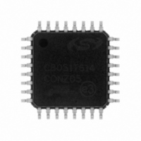
C8051T614-GQ Silicon Laboratories Inc, C8051T614-GQ Datasheet - Page 20
C8051T614-GQ
Manufacturer Part Number
C8051T614-GQ
Description
IC 8051 MCU 8K BYTE-PROG 32-LQFP
Manufacturer
Silicon Laboratories Inc
Series
C8051T61xr
Specifications of C8051T614-GQ
Program Memory Type
OTP
Program Memory Size
8KB (8K x 8)
Package / Case
32-LQFP
Core Processor
8051
Core Size
8-Bit
Speed
25MHz
Connectivity
SMBus (2-Wire/I²C), SPI, UART/USART
Peripherals
POR, PWM, WDT
Number Of I /o
29
Ram Size
1.25K x 8
Voltage - Supply (vcc/vdd)
1.8 V ~ 3.6 V
Oscillator Type
Internal
Operating Temperature
-40°C ~ 85°C
Processor Series
C8051T6x
Core
8051
Data Bus Width
8 bit
Data Ram Size
1.25 KB
Interface Type
I2C/SPI/UART
Maximum Clock Frequency
25 MHz
Number Of Programmable I/os
29
Number Of Timers
4
Maximum Operating Temperature
+ 85 C
Mounting Style
SMD/SMT
3rd Party Development Tools
PK51, CA51, A51, ULINK2
Development Tools By Supplier
C8051FT610DK
Minimum Operating Temperature
- 40 C
On-chip Adc
21-ch x 10-bit
Package
32LQFP
Device Core
8051
Family Name
C8051T61x
Maximum Speed
25 MHz
Operating Supply Voltage
2.5|3.3 V
Lead Free Status / RoHS Status
Lead free / RoHS Compliant
Eeprom Size
-
Data Converters
-
Lead Free Status / Rohs Status
Lead free / RoHS Compliant
Other names
336-1441
Available stocks
Company
Part Number
Manufacturer
Quantity
Price
Company:

Part Number:
C8051T614-GQ
Manufacturer:
Silicon
Quantity:
1 500
Company:
Part Number:
C8051T614-GQ
Manufacturer:
Silicon Laboratories Inc
Quantity:
10 000
Company:
Part Number:
C8051T614-GQR
Manufacturer:
Silicon Laboratories Inc
Quantity:
10 000


C8051T610/1/2/3/4/5/6/7
3. Pin Definitions
Table 3.1. Pin Definitions for the C8051T610/1/2/3/4/5/6/7
20
Name
V
GND
RST/
C2CK
P3.0/
C2D
P0.0
P0.1
P0.2/
VPP
P0.3
P0.4
P0.5
P0.6
P0.7
P1.0
P1.1
P1.2
DD
T610/2/4
Pin
32
31
30
29
28
27
26
25
24
4
3
5
6
2
1
T611/3/5
Pin
28
27
26
25
24
23
22
21
20
4
3
5
6
2
1
T616/7
Pin
24
23
22
21
20
19
18
17
16
4
3
5
6
2
1
Type
D I/O
D I/O
D I/O or
A In
D I/O
D I/O or
A In
D I/O or
A In
D I/O or
A In
A In
D I/O or
A in
D I/O or
A In
D I/O or
A In
D I/O or
A In
D I/O
D I/O or
A In
D I/O or
A In
D I/O or
A In
Rev 1.0
Description
Power Supply Voltage.
Ground.
Device Reset. Open-drain output of internal POR.
Clock signal for the C2 Debug Interface.
Port 3.0.
Bi-directional data signal for the C2 Debug Inter-
face.
Port 0.0.
Port 0.1.
Port 0.2.
VPP Programming Voltage Input.
Port 0.3.
Port 0.4.
Port 0.5.
Port 0.6.
Port 0.7.
Port 1.0.
Port 1.1.
Port 1.2.
Related parts for C8051T614-GQ
Image
Part Number
Description
Manufacturer
Datasheet
Request
R

Part Number:
Description:
SMD/C°/SINGLE-ENDED OUTPUT SILICON OSCILLATOR
Manufacturer:
Silicon Laboratories Inc
Part Number:
Description:
Manufacturer:
Silicon Laboratories Inc
Datasheet:
Part Number:
Description:
N/A N/A/SI4010 AES KEYFOB DEMO WITH LCD RX
Manufacturer:
Silicon Laboratories Inc
Datasheet:
Part Number:
Description:
N/A N/A/SI4010 SIMPLIFIED KEY FOB DEMO WITH LED RX
Manufacturer:
Silicon Laboratories Inc
Datasheet:
Part Number:
Description:
N/A/-40 TO 85 OC/EZLINK MODULE; F930/4432 HIGH BAND (REV E/B1)
Manufacturer:
Silicon Laboratories Inc
Part Number:
Description:
EZLink Module; F930/4432 Low Band (rev e/B1)
Manufacturer:
Silicon Laboratories Inc
Part Number:
Description:
I°/4460 10 DBM RADIO TEST CARD 434 MHZ
Manufacturer:
Silicon Laboratories Inc
Part Number:
Description:
I°/4461 14 DBM RADIO TEST CARD 868 MHZ
Manufacturer:
Silicon Laboratories Inc
Part Number:
Description:
I°/4463 20 DBM RFSWITCH RADIO TEST CARD 460 MHZ
Manufacturer:
Silicon Laboratories Inc
Part Number:
Description:
I°/4463 20 DBM RADIO TEST CARD 868 MHZ
Manufacturer:
Silicon Laboratories Inc
Part Number:
Description:
I°/4463 27 DBM RADIO TEST CARD 868 MHZ
Manufacturer:
Silicon Laboratories Inc
Part Number:
Description:
I°/4463 SKYWORKS 30 DBM RADIO TEST CARD 915 MHZ
Manufacturer:
Silicon Laboratories Inc
Part Number:
Description:
N/A N/A/-40 TO 85 OC/4463 RFMD 30 DBM RADIO TEST CARD 915 MHZ
Manufacturer:
Silicon Laboratories Inc
Part Number:
Description:
I°/4463 20 DBM RADIO TEST CARD 169 MHZ
Manufacturer:
Silicon Laboratories Inc