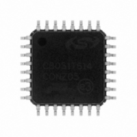
C8051T614-GQ Silicon Laboratories Inc, C8051T614-GQ Datasheet - Page 114

C8051T614-GQ
Manufacturer Part Number
C8051T614-GQ
Description
IC 8051 MCU 8K BYTE-PROG 32-LQFP
Manufacturer
Silicon Laboratories Inc
Series
C8051T61xr
Specifications of C8051T614-GQ
Program Memory Type
OTP
Program Memory Size
8KB (8K x 8)
Package / Case
32-LQFP
Core Processor
8051
Core Size
8-Bit
Speed
25MHz
Connectivity
SMBus (2-Wire/I²C), SPI, UART/USART
Peripherals
POR, PWM, WDT
Number Of I /o
29
Ram Size
1.25K x 8
Voltage - Supply (vcc/vdd)
1.8 V ~ 3.6 V
Oscillator Type
Internal
Operating Temperature
-40°C ~ 85°C
Processor Series
C8051T6x
Core
8051
Data Bus Width
8 bit
Data Ram Size
1.25 KB
Interface Type
I2C/SPI/UART
Maximum Clock Frequency
25 MHz
Number Of Programmable I/os
29
Number Of Timers
4
Maximum Operating Temperature
+ 85 C
Mounting Style
SMD/SMT
3rd Party Development Tools
PK51, CA51, A51, ULINK2
Development Tools By Supplier
C8051FT610DK
Minimum Operating Temperature
- 40 C
On-chip Adc
21-ch x 10-bit
Package
32LQFP
Device Core
8051
Family Name
C8051T61x
Maximum Speed
25 MHz
Operating Supply Voltage
2.5|3.3 V
Lead Free Status / RoHS Status
Lead free / RoHS Compliant
Eeprom Size
-
Data Converters
-
Lead Free Status / Rohs Status
Lead free / RoHS Compliant
Other names
336-1441
Available stocks
Company
Part Number
Manufacturer
Quantity
Price
Company:
Part Number:
C8051T614-GQ
Manufacturer:
Silicon
Quantity:
1 500
Company:
Part Number:
C8051T614-GQ
Manufacturer:
Silicon Laboratories Inc
Quantity:
10 000
Company:
Part Number:
C8051T614-GQR
Manufacturer:
Silicon Laboratories Inc
Quantity:
10 000
C8051T610/1/2/3/4/5/6/7
21.1. Port I/O Modes of Operation
Port pins use the Port I/O cell shown in Figure 21.2. Each Port I/O cell can be configured by software for
analog I/O or digital I/O using the PnMDIN registers. On reset, all Port I/O cells default to a high impedance
state with weak pull-ups enabled until the Crossbar is enabled (XBARE = 1).
21.1.1. Port Pins Configured for Analog I/O
Any pins to be used as Comparator or ADC input, external oscillator input/output, or VREF should be con-
figured for analog I/O (PnMDIN.n = 1). When a pin is configured for analog I/O, its weak pullup, digital
driver, and digital receiver are disabled. Port pins configured for analog I/O will always read back a value of
0.
Configuring pins as analog I/O saves power and isolates the Port pin from digital interference. Port pins
configured as digital inputs may still be used by analog peripherals; however, this practice is not recom-
mended and may result in measurement errors.
21.1.2. Port Pins Configured For Digital I/O
Any pins to be used by digital peripherals (UART, SPI, SMBus, etc.), external digital event capture func-
tions, or as GPIO should be configured as digital I/O (PnMDIN.n = 1). For digital I/O pins, one of two output
modes (push-pull or open-drain) must be selected using the PnMDOUT registers.
Push-pull outputs (PnMDOUT.n = 1) drive the Port pad to the VDD or GND supply rails based on the out-
put logic value of the Port pin. Open-drain outputs have the high side driver disabled; therefore, they only
drive the Port pad to GND when the output logic value is 0 and become high impedance inputs (both high
low drivers turned off) when the output logic value is 1.
When a digital I/O cell is placed in the high impedance state, a weak pull-up transistor pulls the Port pad to
the VDD supply voltage to ensure the digital input is at a defined logic state. Weak pull-ups are disabled
when the I/O cell is driven to GND to minimize power consumption and may be globally disabled by setting
WEAKPUD to 1. The user should ensure that digital I/O are always internally or externally pulled or driven
to a valid logic state to minimize power consumption. Port pins configured for digital I/O always read back
the logic state of the Port pad, regardless of the output logic value of the Port pin.
114
Rev 1.0


