C8051F300-GM Silicon Laboratories Inc, C8051F300-GM Datasheet - Page 84
C8051F300-GM
Manufacturer Part Number
C8051F300-GM
Description
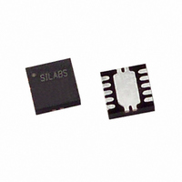
IC 8051 MCU 8K FLASH 11QFN
Manufacturer
Silicon Laboratories Inc
Series
C8051F30xr
Datasheets
1.DTMFDECODER-RD.pdf
(178 pages)
2.C8051F300-TB.pdf
(2 pages)
3.C8051F300-GM.pdf
(174 pages)
Specifications of C8051F300-GM
Program Memory Type
FLASH
Program Memory Size
8KB (8K x 8)
Package / Case
11-VQFN
Core Processor
8051
Core Size
8-Bit
Speed
25MHz
Connectivity
SMBus (2-Wire/I²C), UART/USART
Peripherals
POR, PWM, Temp Sensor, WDT
Number Of I /o
8
Ram Size
256 x 8
Voltage - Supply (vcc/vdd)
2.7 V ~ 3.6 V
Data Converters
A/D 8x8b
Oscillator Type
Internal
Operating Temperature
-40°C ~ 85°C
Processor Series
C8051F3x
Core
8051
Data Bus Width
8 bit
Data Ram Size
256 B
Interface Type
I2C, SMBus, UART
Maximum Clock Frequency
25 MHz
Number Of Programmable I/os
8
Number Of Timers
3 bit
Operating Supply Voltage
2.7 V to 3.6 V
Maximum Operating Temperature
+ 85 C
Mounting Style
SMD/SMT
3rd Party Development Tools
PK51, CA51, A51, ULINK2
Development Tools By Supplier
C8051F226DK
Minimum Operating Temperature
- 40 C
On-chip Adc
8 bit, 8 Channel
No. Of I/o's
8
Ram Memory Size
256Byte
Cpu Speed
25MHz
No. Of Timers
3
Rohs Compliant
Yes
Package
11QFN EP
Device Core
8051
Family Name
C8051F30x
Maximum Speed
25 MHz
Lead Free Status / RoHS Status
Lead free / RoHS Compliant
For Use With
770-1006 - ISP 4PORT FOR SILABS C8051F MCU336-1444 - ADAPTER PROGRAM TOOLSTICK F300336-1351 - KIT REF DES TEMP COMPENS RTC336-1348 - KIT STARTER TOOLSTICK336-1283 - KIT REF DESIGN DTMF DECODER336-1278 - KIT TOOL EVAL SYS IN A USB STICK336-1246 - DEV KIT F300/301/302/303/304/305
Eeprom Size
-
Lead Free Status / Rohs Status
Lead free / RoHS Compliant
Other names
336-1245
Available stocks
Company
Part Number
Manufacturer
Quantity
Price
Company:

Part Number:
C8051F300-GM
Manufacturer:
SiliconL
Quantity:
1 888
Company:
Part Number:
C8051F300-GM
Manufacturer:
TST
Quantity:
5 000
Part Number:
C8051F300-GMR
Manufacturer:
SILICON LABS/芯科
Quantity:
20 000


C8051F300/1/2/3/4/5
9.7.
If a Flash read/write/erase or program read targets an illegal address, a system reset is generated. This
may occur due to any of the following:
•
•
•
The FERROR bit (RSTSRC.6) is set following a Flash error reset. The state of the /RST pin is unaffected
by this reset.
9.8.
Software may force a reset by writing a ‘1’ to the SWRSF bit (RSTSRC.4). The SWRSF bit will read ‘1’ fol-
lowing a software forced reset. The state of the /RST pin is unaffected by this reset.
84
–40 to +85 °C unless otherwise specified.
Missing Clock Detector Timeout Time from last system clock rising
V
/RST Input Leakage Current
Minimum /RST Low Time to
DD
Generate a System Reset
/RST Output Low Voltage
A Flash write or erase is attempted above user code space. This occurs when PSWE is set to ‘1’ and a
MOVX operation is attempted above the user code space address limit.
A Flash read is attempted above user code space. This occurs when a MOVC operation is attempted
above the user code space address limit.
A Program read is attempted above user code space. This occurs when user code attempts to branch
to an address above the user code space address limit.
/RST Input High Voltage
/RST Input Low Voltage
Monitor Threshold (V
Reset Time Delay
Flash Error Reset
Software Reset
V
DD
Parameter
Ramp Time
C8051F300/1/2/3
Table 9.1. User Code Space Address Limits
C8051F304
C8051F305
Table 9.2. Reset Electrical Characteristics
RST
Device
)
I
OL
reset source and code execution
Delay between release of any
= 8.5 mA, V
edge to reset initiation
at location 0x0000
V
/RST = 0.0 V
DD
Conditions
User Code Space Address Limit
= 0 to V
Rev. 2.6
DD
= 2.7 V to 3.6 V
RST
0x1DFF
0x0FFF
0x07FF
0.7 x V
2.40
Min
100
5.0
15
—
DD
2.55
Typ
220
25
—
0.3 x V
Max
2.70
500
0.6
40
1
DD
Units
ms
µA
µs
µs
µs
V
V
V
Related parts for C8051F300-GM
Image
Part Number
Description
Manufacturer
Datasheet
Request
R

Part Number:
Description:
SMD/C°/SINGLE-ENDED OUTPUT SILICON OSCILLATOR
Manufacturer:
Silicon Laboratories Inc
Part Number:
Description:
Manufacturer:
Silicon Laboratories Inc
Datasheet:
Part Number:
Description:
N/A N/A/SI4010 AES KEYFOB DEMO WITH LCD RX
Manufacturer:
Silicon Laboratories Inc
Datasheet:
Part Number:
Description:
N/A N/A/SI4010 SIMPLIFIED KEY FOB DEMO WITH LED RX
Manufacturer:
Silicon Laboratories Inc
Datasheet:
Part Number:
Description:
N/A/-40 TO 85 OC/EZLINK MODULE; F930/4432 HIGH BAND (REV E/B1)
Manufacturer:
Silicon Laboratories Inc
Part Number:
Description:
EZLink Module; F930/4432 Low Band (rev e/B1)
Manufacturer:
Silicon Laboratories Inc
Part Number:
Description:
I°/4460 10 DBM RADIO TEST CARD 434 MHZ
Manufacturer:
Silicon Laboratories Inc
Part Number:
Description:
I°/4461 14 DBM RADIO TEST CARD 868 MHZ
Manufacturer:
Silicon Laboratories Inc
Part Number:
Description:
I°/4463 20 DBM RFSWITCH RADIO TEST CARD 460 MHZ
Manufacturer:
Silicon Laboratories Inc
Part Number:
Description:
I°/4463 20 DBM RADIO TEST CARD 868 MHZ
Manufacturer:
Silicon Laboratories Inc
Part Number:
Description:
I°/4463 27 DBM RADIO TEST CARD 868 MHZ
Manufacturer:
Silicon Laboratories Inc
Part Number:
Description:
I°/4463 SKYWORKS 30 DBM RADIO TEST CARD 915 MHZ
Manufacturer:
Silicon Laboratories Inc
Part Number:
Description:
N/A N/A/-40 TO 85 OC/4463 RFMD 30 DBM RADIO TEST CARD 915 MHZ
Manufacturer:
Silicon Laboratories Inc
Part Number:
Description:
I°/4463 20 DBM RADIO TEST CARD 169 MHZ
Manufacturer:
Silicon Laboratories Inc