C8051F300-GM Silicon Laboratories Inc, C8051F300-GM Datasheet - Page 83
C8051F300-GM
Manufacturer Part Number
C8051F300-GM
Description
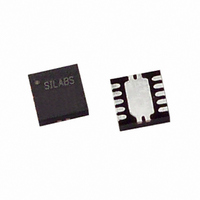
IC 8051 MCU 8K FLASH 11QFN
Manufacturer
Silicon Laboratories Inc
Series
C8051F30xr
Datasheets
1.DTMFDECODER-RD.pdf
(178 pages)
2.C8051F300-TB.pdf
(2 pages)
3.C8051F300-GM.pdf
(174 pages)
Specifications of C8051F300-GM
Program Memory Type
FLASH
Program Memory Size
8KB (8K x 8)
Package / Case
11-VQFN
Core Processor
8051
Core Size
8-Bit
Speed
25MHz
Connectivity
SMBus (2-Wire/I²C), UART/USART
Peripherals
POR, PWM, Temp Sensor, WDT
Number Of I /o
8
Ram Size
256 x 8
Voltage - Supply (vcc/vdd)
2.7 V ~ 3.6 V
Data Converters
A/D 8x8b
Oscillator Type
Internal
Operating Temperature
-40°C ~ 85°C
Processor Series
C8051F3x
Core
8051
Data Bus Width
8 bit
Data Ram Size
256 B
Interface Type
I2C, SMBus, UART
Maximum Clock Frequency
25 MHz
Number Of Programmable I/os
8
Number Of Timers
3 bit
Operating Supply Voltage
2.7 V to 3.6 V
Maximum Operating Temperature
+ 85 C
Mounting Style
SMD/SMT
3rd Party Development Tools
PK51, CA51, A51, ULINK2
Development Tools By Supplier
C8051F226DK
Minimum Operating Temperature
- 40 C
On-chip Adc
8 bit, 8 Channel
No. Of I/o's
8
Ram Memory Size
256Byte
Cpu Speed
25MHz
No. Of Timers
3
Rohs Compliant
Yes
Package
11QFN EP
Device Core
8051
Family Name
C8051F30x
Maximum Speed
25 MHz
Lead Free Status / RoHS Status
Lead free / RoHS Compliant
For Use With
770-1006 - ISP 4PORT FOR SILABS C8051F MCU336-1444 - ADAPTER PROGRAM TOOLSTICK F300336-1351 - KIT REF DES TEMP COMPENS RTC336-1348 - KIT STARTER TOOLSTICK336-1283 - KIT REF DESIGN DTMF DECODER336-1278 - KIT TOOL EVAL SYS IN A USB STICK336-1246 - DEV KIT F300/301/302/303/304/305
Eeprom Size
-
Lead Free Status / Rohs Status
Lead free / RoHS Compliant
Other names
336-1245
Available stocks
Company
Part Number
Manufacturer
Quantity
Price
Company:

Part Number:
C8051F300-GM
Manufacturer:
SiliconL
Quantity:
1 888
Company:
Part Number:
C8051F300-GM
Manufacturer:
TST
Quantity:
5 000
Part Number:
C8051F300-GMR
Manufacturer:
SILICON LABS/芯科
Quantity:
20 000


monitor is disabled after power-on resets; however its defined state (enabled/disabled) is not altered by
any other reset source. For example, if the V
V
bit in register RSTSRC. See Figure 9.2 for V
after a V
Important Note: Enabling the V
return from the reset state with the V
V
9.3.
The external /RST pin provides a means for external circuitry to force the device into a reset state. Assert-
ing an active-low signal on the /RST pin generates a reset; an external pullup and/or decoupling of the
/RST pin may be necessary to avoid erroneous noise-induced resets. See Table 9.2 for complete /RST pin
specifications. The PINRSF flag (RSTSRC.0) is set on exit from an external reset.
9.4.
The Missing Clock Detector (MCD) is a one-shot circuit that is triggered by the system clock. If the system
clock remains high or low for more than 100 µs, the one-shot will time out and generate a reset. After a
MCD reset, the MCDRSF flag (RSTSRC.2) will read ‘1’, signifying the MCD as the reset source; otherwise,
this bit reads ‘0’. Writing a ‘1’ to the MCDRSF bit enables the Missing Clock Detector; writing a ‘0’ disables
it. The state of the /RST pin is unaffected by this reset.
9.5.
Comparator0 can be configured as a reset source by writing a ‘1’ to the C0RSEF flag (RSTSRC.5).
Comparator0 should be enabled and allowed to settle prior to writing to C0RSEF to prevent any turn-on
chatter on the output from generating an unwanted reset. The Comparator0 reset is active-low: if the non-
inverting input voltage (on CP0+) is less than the inverting input voltage (on CP0–), the device is put into
the reset state. After a Comparator0 reset, the C0RSEF flag (RSTSRC.5) will read ‘1’ signifying
Comparator0 as the reset source; otherwise, this bit reads ‘0’. The state of the /RST pin is unaffected by
this reset.
9.6.
The programmable Watchdog Timer (WDT) function of the Programmable Counter Array (PCA) can be
used to prevent software from running out of control during a system malfunction. The PCA WDT function
can be enabled or disabled by software as described in
page
prevents user software from updating the WDT, a reset is generated and the WDTRSF bit (RSTSRC.5) is
set to ‘1’. The state of the /RST pin is unaffected by this reset.
DD
DD
monitor will still be enabled after the reset. The V
monitor is enabled does not cause a system reset.
160; the WDT is enabled and clocked by SYSCLK / 12 following any reset. If a system malfunction
External Reset
Missing Clock Detector Reset
Comparator0 Reset
PCA Watchdog Timer Reset
DD
monitor reset. See Table 9.2 for electrical characteristics of the V
DD
monitor will immediately generate a system reset. The device will then
DD
monitor enabled. Writing a logic ‘1’ to the PORSF flag when the
DD
DD
monitor is enabled and a software reset is performed, the
Rev. 2.6
monitor timing; note that the reset delay is not incurred
DD
monitor is enabled by writing a ‘1’ to the PORSF
Section “16.3. Watchdog Timer Mode” on
C8051F300/1/2/3/4/5
DD
monitor.
83
Related parts for C8051F300-GM
Image
Part Number
Description
Manufacturer
Datasheet
Request
R

Part Number:
Description:
SMD/C°/SINGLE-ENDED OUTPUT SILICON OSCILLATOR
Manufacturer:
Silicon Laboratories Inc
Part Number:
Description:
Manufacturer:
Silicon Laboratories Inc
Datasheet:
Part Number:
Description:
N/A N/A/SI4010 AES KEYFOB DEMO WITH LCD RX
Manufacturer:
Silicon Laboratories Inc
Datasheet:
Part Number:
Description:
N/A N/A/SI4010 SIMPLIFIED KEY FOB DEMO WITH LED RX
Manufacturer:
Silicon Laboratories Inc
Datasheet:
Part Number:
Description:
N/A/-40 TO 85 OC/EZLINK MODULE; F930/4432 HIGH BAND (REV E/B1)
Manufacturer:
Silicon Laboratories Inc
Part Number:
Description:
EZLink Module; F930/4432 Low Band (rev e/B1)
Manufacturer:
Silicon Laboratories Inc
Part Number:
Description:
I°/4460 10 DBM RADIO TEST CARD 434 MHZ
Manufacturer:
Silicon Laboratories Inc
Part Number:
Description:
I°/4461 14 DBM RADIO TEST CARD 868 MHZ
Manufacturer:
Silicon Laboratories Inc
Part Number:
Description:
I°/4463 20 DBM RFSWITCH RADIO TEST CARD 460 MHZ
Manufacturer:
Silicon Laboratories Inc
Part Number:
Description:
I°/4463 20 DBM RADIO TEST CARD 868 MHZ
Manufacturer:
Silicon Laboratories Inc
Part Number:
Description:
I°/4463 27 DBM RADIO TEST CARD 868 MHZ
Manufacturer:
Silicon Laboratories Inc
Part Number:
Description:
I°/4463 SKYWORKS 30 DBM RADIO TEST CARD 915 MHZ
Manufacturer:
Silicon Laboratories Inc
Part Number:
Description:
N/A N/A/-40 TO 85 OC/4463 RFMD 30 DBM RADIO TEST CARD 915 MHZ
Manufacturer:
Silicon Laboratories Inc
Part Number:
Description:
I°/4463 20 DBM RADIO TEST CARD 169 MHZ
Manufacturer:
Silicon Laboratories Inc