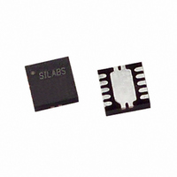
C8051F300-GM Silicon Laboratories Inc, C8051F300-GM Datasheet - Page 82

C8051F300-GM
Manufacturer Part Number
C8051F300-GM
Description
IC 8051 MCU 8K FLASH 11QFN
Manufacturer
Silicon Laboratories Inc
Series
C8051F30xr
Datasheets
1.DTMFDECODER-RD.pdf
(178 pages)
2.C8051F300-TB.pdf
(2 pages)
3.C8051F300-GM.pdf
(174 pages)
Specifications of C8051F300-GM
Program Memory Type
FLASH
Program Memory Size
8KB (8K x 8)
Package / Case
11-VQFN
Core Processor
8051
Core Size
8-Bit
Speed
25MHz
Connectivity
SMBus (2-Wire/I²C), UART/USART
Peripherals
POR, PWM, Temp Sensor, WDT
Number Of I /o
8
Ram Size
256 x 8
Voltage - Supply (vcc/vdd)
2.7 V ~ 3.6 V
Data Converters
A/D 8x8b
Oscillator Type
Internal
Operating Temperature
-40°C ~ 85°C
Processor Series
C8051F3x
Core
8051
Data Bus Width
8 bit
Data Ram Size
256 B
Interface Type
I2C, SMBus, UART
Maximum Clock Frequency
25 MHz
Number Of Programmable I/os
8
Number Of Timers
3 bit
Operating Supply Voltage
2.7 V to 3.6 V
Maximum Operating Temperature
+ 85 C
Mounting Style
SMD/SMT
3rd Party Development Tools
PK51, CA51, A51, ULINK2
Development Tools By Supplier
C8051F226DK
Minimum Operating Temperature
- 40 C
On-chip Adc
8 bit, 8 Channel
No. Of I/o's
8
Ram Memory Size
256Byte
Cpu Speed
25MHz
No. Of Timers
3
Rohs Compliant
Yes
Package
11QFN EP
Device Core
8051
Family Name
C8051F30x
Maximum Speed
25 MHz
Lead Free Status / RoHS Status
Lead free / RoHS Compliant
For Use With
770-1006 - ISP 4PORT FOR SILABS C8051F MCU336-1444 - ADAPTER PROGRAM TOOLSTICK F300336-1351 - KIT REF DES TEMP COMPENS RTC336-1348 - KIT STARTER TOOLSTICK336-1283 - KIT REF DESIGN DTMF DECODER336-1278 - KIT TOOL EVAL SYS IN A USB STICK336-1246 - DEV KIT F300/301/302/303/304/305
Eeprom Size
-
Lead Free Status / Rohs Status
Lead free / RoHS Compliant
Other names
336-1245
Available stocks
Company
Part Number
Manufacturer
Quantity
Price
Company:
Part Number:
C8051F300-GM
Manufacturer:
SiliconL
Quantity:
1 888
Company:
Part Number:
C8051F300-GM
Manufacturer:
TST
Quantity:
5 000
Part Number:
C8051F300-GMR
Manufacturer:
SILICON LABS/芯科
Quantity:
20 000
C8051F300/1/2/3/4/5
9.1.
During powerup, the device is held in a reset state and the /RST pin is driven low until V
V
ramp time increases (V
times (less than 1 ms), the power-on reset delay (T
Note: The maximum V
released from reset before V
On exit from a power-on reset, the PORSF flag (RSTSRC.1) is set by hardware to logic 1. When PORSF is
set, all of the other reset flags in the RSTSRC Register are indeterminate (PORSF is cleared by all other
resets). Since all resets cause program execution to begin at the same location (0x0000) software can
read the PORSF flag to determine if a powerup was the cause of reset. The content of internal data mem-
ory should be assumed to be undefined after a power-on reset. The V
power-on reset.
9.2.
When a power-down transition or power irregularity causes V
monitor will drive the /RST pin low and hold the CIP-51 in a reset state (see Figure 9.2). When V
to a level above V
memory contents are not altered by the power-fail reset, it is impossible to determine if V
the level required for data retention. If the PORSF flag reads ‘1’, the data may no longer be valid. The V
82
RST
. An additional delay occurs before the device is released from reset; the delay decreases as the V
Power-On Reset
Power-Fail Reset / V
Logic HIGH
Logic LOW
RST
Figure 9.2. Power-On and V
2.70
2.55
2.0
1.0
, the CIP-51 will be released from the reset state. Note that even though internal data
DD
DD
ramp time is defined as how fast V
/RST
ramp time is 1 ms; slower ramp times may cause the device to be
DD
V
reaches the VRST level.
RST
DD
Monitor
Power-On
Reset
T
PORDelay
Rev. 2.6
PORDelay
DD
Monitor Reset Timing
) is typically less than 0.3 ms.
DD
DD
ramps from 0 V to V
to drop below V
Monitor
Reset
VDD
DD
monitor is disabled following a
RST
VDD
RST
, the power supply
DD
DD
). For valid ramp
t
dropped below
settles above
DD
returns
DD
DD


