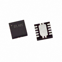
C8051F300-GM Silicon Laboratories Inc, C8051F300-GM Datasheet - Page 109

C8051F300-GM
Manufacturer Part Number
C8051F300-GM
Description
IC 8051 MCU 8K FLASH 11QFN
Manufacturer
Silicon Laboratories Inc
Series
C8051F30xr
Datasheets
1.DTMFDECODER-RD.pdf
(178 pages)
2.C8051F300-TB.pdf
(2 pages)
3.C8051F300-GM.pdf
(174 pages)
Specifications of C8051F300-GM
Program Memory Type
FLASH
Program Memory Size
8KB (8K x 8)
Package / Case
11-VQFN
Core Processor
8051
Core Size
8-Bit
Speed
25MHz
Connectivity
SMBus (2-Wire/I²C), UART/USART
Peripherals
POR, PWM, Temp Sensor, WDT
Number Of I /o
8
Ram Size
256 x 8
Voltage - Supply (vcc/vdd)
2.7 V ~ 3.6 V
Data Converters
A/D 8x8b
Oscillator Type
Internal
Operating Temperature
-40°C ~ 85°C
Processor Series
C8051F3x
Core
8051
Data Bus Width
8 bit
Data Ram Size
256 B
Interface Type
I2C, SMBus, UART
Maximum Clock Frequency
25 MHz
Number Of Programmable I/os
8
Number Of Timers
3 bit
Operating Supply Voltage
2.7 V to 3.6 V
Maximum Operating Temperature
+ 85 C
Mounting Style
SMD/SMT
3rd Party Development Tools
PK51, CA51, A51, ULINK2
Development Tools By Supplier
C8051F226DK
Minimum Operating Temperature
- 40 C
On-chip Adc
8 bit, 8 Channel
No. Of I/o's
8
Ram Memory Size
256Byte
Cpu Speed
25MHz
No. Of Timers
3
Rohs Compliant
Yes
Package
11QFN EP
Device Core
8051
Family Name
C8051F30x
Maximum Speed
25 MHz
Lead Free Status / RoHS Status
Lead free / RoHS Compliant
For Use With
770-1006 - ISP 4PORT FOR SILABS C8051F MCU336-1444 - ADAPTER PROGRAM TOOLSTICK F300336-1351 - KIT REF DES TEMP COMPENS RTC336-1348 - KIT STARTER TOOLSTICK336-1283 - KIT REF DESIGN DTMF DECODER336-1278 - KIT TOOL EVAL SYS IN A USB STICK336-1246 - DEV KIT F300/301/302/303/304/305
Eeprom Size
-
Lead Free Status / Rohs Status
Lead free / RoHS Compliant
Other names
336-1245
Available stocks
Company
Part Number
Manufacturer
Quantity
Price
Company:
Part Number:
C8051F300-GM
Manufacturer:
SiliconL
Quantity:
1 888
Company:
Part Number:
C8051F300-GM
Manufacturer:
TST
Quantity:
5 000
Part Number:
C8051F300-GMR
Manufacturer:
SILICON LABS/芯科
Quantity:
20 000
C8051F300/1/2/3/4/5
The direction bit (R/W) occupies the least significant bit position of the address byte. The direction bit is set
to logic 1 to indicate a "READ" operation and cleared to logic 0 to indicate a "WRITE" operation.
All transactions are initiated by a master, with one or more addressed slave devices as the target. The
master generates the START condition and then transmits the slave address and direction bit. If the trans-
action is a WRITE operation from the master to the slave, the master transmits the data a byte at a time
waiting for an ACK from the slave at the end of each byte. For READ operations, the slave transmits the
data waiting for an ACK from the master at the end of each byte. At the end of the data transfer, the master
generates a STOP condition to terminate the transaction and free the bus. Figure 13.3 illustrates a typical
SMBus transaction.
SCL
SDA
SLA6
SLA5-0
R/W
D7
D6-0
START
Slave Address + R/W
ACK
Data Byte
NACK
STOP
Figure 13.3. SMBus Transaction
13.3.1. Arbitration
A master may start a transfer only if the bus is free. The bus is free after a STOP condition or after the SCL
and SDA lines remain high for a specified time (see
Section “13.3.4. SCL High (SMBus Free) Timeout”
on page
110). In the event that two or more devices attempt to begin a transfer at the same time, an arbi-
tration scheme is employed to force one master to give up the bus. The master devices continue transmit-
ting until one attempts a HIGH while the other transmits a LOW. Since the bus is open-drain, the bus will
be pulled LOW. The master attempting the HIGH will detect a LOW SDA and lose the arbitration. The win-
ning master continues its transmission without interruption; the losing master becomes a slave and
receives the rest of the transfer if addressed. This arbitration scheme is non-destructive: one device
always wins, and no data is lost.
Rev. 2.6
109


