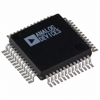
ADUC834BSZ Analog Devices Inc, ADUC834BSZ Datasheet - Page 53

ADUC834BSZ
Manufacturer Part Number
ADUC834BSZ
Description
IC ADC DUAL16/24BIT W/MCU 52MQFP
Manufacturer
Analog Devices Inc
Series
MicroConverter® ADuC8xxr
Specifications of ADUC834BSZ
Core Size
8-Bit
Program Memory Size
62KB (62K x 8)
Oscillator Type
Internal
Core Processor
8052
Speed
12.58MHz
Connectivity
EBI/EMI, I²C, SPI, UART/USART
Peripherals
POR, PSM, PWM, Temp Sensor, WDT
Number Of I /o
34
Program Memory Type
FLASH
Eeprom Size
4K x 8
Ram Size
2.25K x 8
Voltage - Supply (vcc/vdd)
2.7 V ~ 5.25 V
Data Converters
A/D 3x16b, 4x24b; D/A 1x12b
Operating Temperature
-40°C ~ 125°C
Package / Case
52-MQFP, 52-PQFP
Controller Family/series
(8052) ADUC
No. Of I/o's
26
Eeprom Memory Size
62KB
Ram Memory Size
2KB
Cpu Speed
12.58MHz
Package
52MQFP
Device Core
8052
Family Name
ADuC8xx
Maximum Speed
12.58 MHz
Operating Supply Voltage
3.3|5 V
Data Bus Width
8 Bit
Number Of Programmable I/os
26
Interface Type
I2C/SPI/UART
On-chip Adc
4-chx16-bit|4-chx24-bit
On-chip Dac
1-chx12-bit
Number Of Timers
3
Lead Free Status / RoHS Status
Lead free / RoHS Compliant
Available stocks
Company
Part Number
Manufacturer
Quantity
Price
Company:
Part Number:
ADUC834BSZ
Manufacturer:
TOSHIBA
Quantity:
1 200
Company:
Part Number:
ADUC834BSZ
Manufacturer:
Analog Devices Inc
Quantity:
10 000
Part Number:
ADUC834BSZ
Manufacturer:
ADI/亚德诺
Quantity:
20 000
TCON
SFR Address
Power-On Default Value
Bit Addressable
Bit
7
6
5
4
3
2
1
0
*These bits are not used in the control of timer/counter 0 and 1, but are used instead in the control and monitoring of the external INT0 and INT1 interrupt pins.
Timer/Counter 0 and 1 Data Registers
Both timer 0 and timer 1 consist of two 8-bit registers. These can be used as independent registers or combined to be a single 16-bit
register, depending on the timer mode configuration.
TH0 and TL0
Timer 0 high byte and low byte. SFR Address = 8CH, 8AH, respectively.
TH1 and TL1
Timer 1 high byte and low byte. SFR Address = 8DH, 8BH, respectively.
REV. A
Name
TF1
TR1
TF0
TR0
IE1*
IT1*
IE0*
IT0*
Timer/Counter 0 and 1 Control Register
Description
Timer 1 Overflow Flag.
Set by hardware on a Timer/Counter 1 overflow.
Cleared by hardware when the Program Counter (PC) vectors to the interrupt service routine.
Timer 1 Run Control Bit.
Set by user to turn on Timer/Counter 1.
Cleared by user to turn off Timer/Counter 1.
Timer 0 Overflow Flag.
Set by hardware on a Timer/Counter 0 overflow.
Cleared by hardware when the PC vectors to the interrupt service routine.
Timer 0 Run Control Bit.
Set by user to turn on Timer/Counter 0.
Cleared by user to turn off Timer/Counter 0.
External Interrupt 1 (INT1) Flag.
Set by hardware by a falling edge or zero level being applied to external interrupt pin INT1,
depending on bit IT1 state.
Cleared by hardware when the PC vectors to the interrupt service routine only if the interrupt
was transition-activated. If level-activated, the external requesting source controls the
request flag, rather than the on-chip hardware.
External Interrupt 1 (IE1) Trigger Type.
Set by software to specify edge-sensitive detection (i.e., 1-to-0 transition).
Cleared by software to specify level-sensitive detection (i.e., zero level).
External Interrupt 0 (INT0) Flag.
Set by hardware by a falling edge or zero level being applied to external interrupt pin INT0, depending
on bit IT0 state.
Cleared by hardware when the PC vectors to the interrupt service routine only if the interrupt was
transition-activated. If level-activated, the external requesting source controls the request flag,
rather than the on-chip hardware.
External Interrupt 0 (IE0) Trigger Type.
Set by software to specify edge-sensitive detection (i.e., 1-to-0 transition).
Cleared by software to specify level-sensitive detection (i.e., zero level).
88H
00H
Yes
Table XXVII. TCON SFR Bit Designations
–53–
ADuC834


