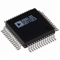
ADUC834BSZ Analog Devices Inc, ADUC834BSZ Datasheet - Page 22

ADUC834BSZ
Manufacturer Part Number
ADUC834BSZ
Description
IC ADC DUAL16/24BIT W/MCU 52MQFP
Manufacturer
Analog Devices Inc
Series
MicroConverter® ADuC8xxr
Specifications of ADUC834BSZ
Core Size
8-Bit
Program Memory Size
62KB (62K x 8)
Oscillator Type
Internal
Core Processor
8052
Speed
12.58MHz
Connectivity
EBI/EMI, I²C, SPI, UART/USART
Peripherals
POR, PSM, PWM, Temp Sensor, WDT
Number Of I /o
34
Program Memory Type
FLASH
Eeprom Size
4K x 8
Ram Size
2.25K x 8
Voltage - Supply (vcc/vdd)
2.7 V ~ 5.25 V
Data Converters
A/D 3x16b, 4x24b; D/A 1x12b
Operating Temperature
-40°C ~ 125°C
Package / Case
52-MQFP, 52-PQFP
Controller Family/series
(8052) ADUC
No. Of I/o's
26
Eeprom Memory Size
62KB
Ram Memory Size
2KB
Cpu Speed
12.58MHz
Package
52MQFP
Device Core
8052
Family Name
ADuC8xx
Maximum Speed
12.58 MHz
Operating Supply Voltage
3.3|5 V
Data Bus Width
8 Bit
Number Of Programmable I/os
26
Interface Type
I2C/SPI/UART
On-chip Adc
4-chx16-bit|4-chx24-bit
On-chip Dac
1-chx12-bit
Number Of Timers
3
Lead Free Status / RoHS Status
Lead free / RoHS Compliant
Available stocks
Company
Part Number
Manufacturer
Quantity
Price
Company:
Part Number:
ADUC834BSZ
Manufacturer:
TOSHIBA
Quantity:
1 200
Company:
Part Number:
ADUC834BSZ
Manufacturer:
Analog Devices Inc
Quantity:
10 000
Part Number:
ADUC834BSZ
Manufacturer:
ADI/亚德诺
Quantity:
20 000
ADuC834
PRIMARY AND AUXILIARY ADC NOISE
PERFORMANCE
Tables X, XI, and XII show the output rms noise in V and
output peak-to-peak resolution in bits (rounded to the nearest
0.5 LSB) for some typical output update rates on both the primary
and auxiliary ADCs. The numbers are typical and are generated
at a differential input voltage of 0 V. The output update rate is
SF
Word
13
69
255
SF
Word
13
69
255
SF
Word
13
69
255
*Based on a six-sigma limit, the rms resolution is 2.7 bits greater than the peak-to-peak resolution.
SF
Word
13
69
255
*ADC converting in Bipolar mode
Typical Output RMS Noise vs. Update Rate*
Data Update
Rate (Hz)
105.3
19.79
5.35
Data Update
Rate (Hz)
105.3
19.79
5.35
Data Update
Rate (Hz)
105.3
19.79
5.35
Peak-to-Peak Resolution vs. Input Range and Update Rate; Peak-to-Peak Resolution in Bits
Output RMS Noise in V
Data
R
105.3
19.79
5.35
Typical Output RMS Noise vs. Input Range and Update Rate; Output RMS Noise in V
ate (Hz)
Typical RMS Resolution vs. Input Range and Update Rate: RMS Resolution in Bits*
Update
1.50
0.60
0.35
12
13.5
14
14.7
16.2
16.7
20 mV
20 mV
20 mV
Table X. Primary ADC, Typical Output RMS Noise ( V)
Table XI. Primary ADC, Peak-to-Peak Resolution (Bits)
1.50
0.65
0.35
13
14
15
15.7
16.7
17.7
Input Range
2.5 V
10.75
2.00
1.15
40 mV
40 mV
40 mV
Table XII. Auxiliary ADC
1.60
0.65
0.37
14
15
16
16.7
17.7
18.7
80 mV
80 mV
80 mV
–22–
selected via the Sinc Filter (SF) SFR. It is important to note
that the peak-to-peak resolution figures represent the resolution
for which there will be no code flicker within a six-sigma limit.
The QuickStart Development system PC software comes
complete with an ADC noise evaluation tool. This tool can be
easily used with the evaluation board to see these figures from
silicon.
Input Range
1.75
0.65
0.37
Input Range
15
16
17
Input Range
17.7
18.7
19.7
SF
Word
13
69
255
NOTES
1
2
ADC converting in Bipolar mode
In Unipolar mode, peak-to-peak resolution at 105 Hz is 15 bits.
160 mV
160 mV
160 mV
Peak-to-Peak Resolution vs. Update Rate
Peak-to-Peak Resolution in Bits
3.50
0.65
0.37
15
17
18
17.7
19.7
20.7
320 mV
320 mV
320 mV
Data Update
Rate (Hz)
105.3
19.79
5.35
4.50
0.95
0.51
15.5
17.5
18.5
18.2
20.2
21.2
640 mV
640 mV
640 mV
6.70
1.40
0.82
16
18
19
18.7
20.7
21.7
16
16
16
Input Range
2.5 V
1.28 V
1.28 V
1.28 V
2
1
16
18.5
19.5
18.7
21.2
22.2
REV. A
11.75
2.30
1.25
2.56 V
2.56 V
2.56 V


