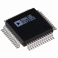
ADUC834BSZ Analog Devices Inc, ADUC834BSZ Datasheet - Page 51

ADUC834BSZ
Manufacturer Part Number
ADUC834BSZ
Description
IC ADC DUAL16/24BIT W/MCU 52MQFP
Manufacturer
Analog Devices Inc
Series
MicroConverter® ADuC8xxr
Specifications of ADUC834BSZ
Core Size
8-Bit
Program Memory Size
62KB (62K x 8)
Oscillator Type
Internal
Core Processor
8052
Speed
12.58MHz
Connectivity
EBI/EMI, I²C, SPI, UART/USART
Peripherals
POR, PSM, PWM, Temp Sensor, WDT
Number Of I /o
34
Program Memory Type
FLASH
Eeprom Size
4K x 8
Ram Size
2.25K x 8
Voltage - Supply (vcc/vdd)
2.7 V ~ 5.25 V
Data Converters
A/D 3x16b, 4x24b; D/A 1x12b
Operating Temperature
-40°C ~ 125°C
Package / Case
52-MQFP, 52-PQFP
Controller Family/series
(8052) ADUC
No. Of I/o's
26
Eeprom Memory Size
62KB
Ram Memory Size
2KB
Cpu Speed
12.58MHz
Package
52MQFP
Device Core
8052
Family Name
ADuC8xx
Maximum Speed
12.58 MHz
Operating Supply Voltage
3.3|5 V
Data Bus Width
8 Bit
Number Of Programmable I/os
26
Interface Type
I2C/SPI/UART
On-chip Adc
4-chx16-bit|4-chx24-bit
On-chip Dac
1-chx12-bit
Number Of Timers
3
Lead Free Status / RoHS Status
Lead free / RoHS Compliant
Available stocks
Company
Part Number
Manufacturer
Quantity
Price
Company:
Part Number:
ADUC834BSZ
Manufacturer:
TOSHIBA
Quantity:
1 200
Company:
Part Number:
ADUC834BSZ
Manufacturer:
Analog Devices Inc
Quantity:
10 000
Part Number:
ADUC834BSZ
Manufacturer:
ADI/亚德诺
Quantity:
20 000
Notice also that direct access to the SCLOCK and SDATA/MOSI
pins is afforded through the SFR interface in I
Therefore, if you are not using the SPI or I
use these two pins to give additional high current digital outputs.
REV. A
Figure 44. SDATA/MOSI Pin I/O Functional Equivalent
in SPI Mode
Figure 45. SDATA/MOSI Pin I/O Functional Equivalent
in I
Figure 42. SCLOCK Pin I/O Functional Equivalent in
SPI Mode
Figure 43. SCLOCK Pin I/O Functional Equivalent in
I
BITS
SFR
2
SPE = 0 (I
C Mode
(MASTER/SLAVE)
HARDWARE SPI
MDO
MDE
I2CM
2
MDI
(MASTER/SLAVE)
C Mode
HARDWARE SPI
HARDWARE I
(SLAVE ONLY)
SPE = 0 (I
HARDWARE I
(SLAVE ONLY)
I2CM
BITS
MCO
SFR
SPE = 1 (SPI ENABLE)
2
C ENABLE)
SPE = 1 (SPI ENABLE)
2
C ENABLE)
REJECTION FILTER
2
REJECTION FILTER
C
2
C
50ns GLITCH
50ns GLITCH
TRIGGER
SCHMITT
Q1
Q3
Q1
Q3
DV
DV
DV
DD
Q1
(OFF)
Q3
DD
DD
2
C functions, you can
Q2 (OFF)
Q4 (OFF)
Q2 (OFF)
Q4 (OFF)
Q2
Q4
DV
2
Q1
(OFF)
Q3
C master mode.
SCLOCK
DD
PIN
SDATA/
Q2
Q4
SCLOCK
MOSI
PIN
PIN
SDATA/
MOSI
PIN
–51–
As shown in Figure 46, the MISO pin in SPI master/slave
operation offers the exact same pull-up and pull-down configu-
ration as the MOSI pin in SPI slave/master operation.
The SS pin has a weak internal pull-up permanently enabled to
prevent the SS input from floating. This pull-up can be easily
overdriven by an external device to drive the SS pin low.
Read-Modify-Write Instructions
Some 8051 instructions that read a port read the latch and
others read the pin. The instructions that read the latch rather
than the pins are the ones that read a value, possibly change it,
and then rewrite it to the latch. These are called “read-modify-
write” instructions. Listed below are the read-modify-write
instructions. When the destination operand is a port, or a port
bit, these instructions read the latch rather than the pin.
ANL
ORL
XRL
JBC
CPL
INC
DEC
DJNZ
MOV PX.Y, C* (Move Carry to Bit Y of Port X)
CLR PX.Y*
SETB PX.Y*
The reason that read-modify-write instructions are directed to
the latch rather than the pin is to avoid a possible misinterpreta-
tion of the voltage level of a pin. For example, a port pin might
be used to drive the base of a transistor. When a 1 is written to
the bit, the transistor is turned on. If the CPU then reads the
same port bit at the pin rather then the latch, it will read the
base voltage of the transistor and interpret it as a Logic 0. Read-
ing the latch rather than the pin will return the correct value of 1.
*These instruction read the port byte (all 8 bits), modify the addressed bit and
then write the new byte back to the latch.
Figure 46. MISO Pin I/O Functional Equivalent
Figure 47. SS Pin I/O Functional Equivalent
(MASTER/SLAVE)
(MASTER/SLAVE)
HARDWARE SPI
HARDWARE SPI
(Logical AND, e.g., ANL P1, A)
(Logical OR, e.g., ORL P2, A)
(Logical EX-OR, e.g., XRL P3, A)
(Jump If Bit = 1 and Clear Bit,
e.g., JBC P1.1, LABEL
(Complement Bit, e.g., CPL P3.0)
(Increment, e.g., INC P2)
(Decrement, e.g., DEC P2)
(Decrement and Jump IFf Not Zero,
e.g.,DJNZ P3, LABEL)
(Clear Bit Y of Port X)
(Set Bit Y of Port X)
DV
DV
DD
DD
MISO
PIN
SS
PIN
ADuC834


