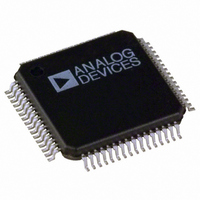
ADUC7024BSTZ62 Analog Devices Inc, ADUC7024BSTZ62 Datasheet - Page 80

ADUC7024BSTZ62
Manufacturer Part Number
ADUC7024BSTZ62
Description
IC MCU FLASH 62K ANLG I/O 64LQFP
Manufacturer
Analog Devices Inc
Series
MicroConverter® ADuC7xxxr
Specifications of ADUC7024BSTZ62
Core Size
16/32-Bit
Program Memory Size
62KB (62K x 8)
Design Resources
Sensing Low-g Acceleration Using ADXL345 Digital Accelerometer Connected to ADuC7024 (CN0133)
Core Processor
ARM7
Speed
44MHz
Connectivity
EBI/EMI, I²C, SPI, UART/USART
Peripherals
PLA, PWM, PSM, Temp Sensor, WDT
Number Of I /o
30
Program Memory Type
FLASH
Ram Size
8K x 8
Voltage - Supply (vcc/vdd)
2.7 V ~ 3.6 V
Data Converters
A/D 10x12b; D/A 2x12b
Oscillator Type
Internal
Operating Temperature
-40°C ~ 125°C
Package / Case
64-LQFP
Controller Family/series
(ARM7) ADUC
No. Of I/o's
30
Ram Memory Size
8KB
Cpu Speed
44MHz
No. Of Timers
4
Digital Ic Case Style
LQFP
Embedded Interface Type
I2C, SPI, UART
Rohs Compliant
Yes
Package
64LQFP
Device Core
ARM7TDMI
Family Name
ADuC7xxx
Maximum Speed
44 MHz
Operating Supply Voltage
3.3 V
Data Bus Width
16|32 Bit
Number Of Programmable I/os
30
Interface Type
I2C/SPI/UART
On-chip Adc
10-chx12-bit
On-chip Dac
2-chx12-bit
Number Of Timers
4
Lead Free Status / RoHS Status
Lead free / RoHS Compliant
Eeprom Size
-
Lead Free Status / RoHS Status
Lead free / RoHS Compliant, Lead free / RoHS Compliant
Available stocks
Company
Part Number
Manufacturer
Quantity
Price
Company:
Part Number:
ADUC7024BSTZ62
Manufacturer:
AD
Quantity:
261
Company:
Part Number:
ADUC7024BSTZ62
Manufacturer:
ADI
Quantity:
248
Company:
Part Number:
ADUC7024BSTZ62
Manufacturer:
Analog Devices Inc
Quantity:
10 000
Part Number:
ADUC7024BSTZ62
Manufacturer:
ADI/亚德诺
Quantity:
20 000
Company:
Part Number:
ADUC7024BSTZ62-RL
Manufacturer:
VISHAY
Quantity:
120
Company:
Part Number:
ADUC7024BSTZ62-RL
Manufacturer:
Analog Devices Inc
Quantity:
10 000
ADuC7019/20/21/22/24/25/26/27/28
Secure Clear Bit (Watchdog Mode Only)
The secure clear bit is provided for a higher level of protection.
When set, a specific sequential value must be written to T3CLRI
to avoid a watchdog reset. The value is a sequence generated
by the 8-bit linear feedback shift register (LFSR) polynomial =
X8 + X6 + X5 + X + 1 as shown in Figure 68.
CLOCK
The initial value or seed is written to T3CLRI before entering
watchdog mode. After entering watchdog mode, a write to
T3CLRI must match this expected value. If it matches, the LFSR
is advanced to the next state when the counter reload happens.
If it fails to match the expected state, a reset is immediately
generated, even if the count has not yet expired.
The value 0x00 should not be used as an initial seed due to the
properties of the polynomial. The value 0x00 is always
guaranteed to force an immediate reset. The value of the LFSR
cannot be read; it must be tracked/generated in software.
Example of a sequence:
1.
2.
3.
4.
5.
EXTERNAL MEMORY INTERFACING
The ADuC7026 and ADuC7027 are the only models in their
series that feature an external memory interface. The external
memory interface requires a larger number of pins. This is why
it is only available on larger pin count packages. The XMCFG
MMR must be set to 1 to use the external port.
Although 32-bit addresses are supported internally, only the
lower 16 bits of the address are on external pins.
The memory interface can address up to four 128 kB of
asynchronous memory (SRAM or/and EEPROM).
The pins required for interfacing to an external memory are
shown in Table 79.
Q
Enter initial seed, 0xAA, in T3CLRI before starting Timer3
in watchdog mode.
Enter 0xAA in T3CLRI; Timer3 is reloaded.
Enter 0x37 in T3CLRI; Timer3 is reloaded.
Enter 0x6E in T3CLRI; Timer3 is reloaded.
Enter 0x66. 0xDC was expected; the watchdog resets the chip.
7
D
Q
6
D
Q
5
D
Figure 68. 8-Bit LFSR
Q
4
D
Q
3
D
Q
2
D
Q
1
D
Q
0
Rev. B | Page 80 of 92
D
Table 79. External Memory Interfacing Pins
Pin
AD[15:0]
A16
MS[3:0]
WS
RS
AE
BHE, BLE
There are four external memory regions available as described
in Table 80. Associated with each region are the MS[3:0] pins.
These signals allow access to the particular region of external
memory. The size of each memory region can be 128 kB maxi-
mum, 64 k × 16 or 128 k × 8. To access 128 k with an 8-bit
memory, an extra address line (A16) is provided. (See the example
in Figure 69). The four regions are configured independently.
Table 80. Memory Regions
Address Start
0x10000000
0x20000000
0x30000000
0x40000000
Each external memory region can be controlled through three
MMRs: XMCFG, XMxCON, and XMxPAR.
ADuC7026/
ADuC7027
AD15:AD0
Figure 69. Interfacing to External EEPROM/RAM
Function
Address/Data Bus.
Extended Addressing for 8-Bit Memory Only.
Memory Select.
Write Strobe.
Read Strobe.
Address Latch Enable.
Byte Write Capability.
MS0
MS1
A16
WS
AE
RS
Address End
0x1000FFFF
0x2000FFFF
0x3000FFFF
0x4000FFFF
LATCH
Contents
External Memory 0
External Memory 1
External Memory 2
External Memory 3
D0:D15
A0:A15
CS
WE
OE
D0:D7
A16
A0:A15
CS
WE
OE
64k × 16-BIT
128k × 8-BIT
EEPROM
RAM


