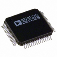
ADUC7024BSTZ62 Analog Devices Inc, ADUC7024BSTZ62 Datasheet - Page 44

ADUC7024BSTZ62
Manufacturer Part Number
ADUC7024BSTZ62
Description
IC MCU FLASH 62K ANLG I/O 64LQFP
Manufacturer
Analog Devices Inc
Series
MicroConverter® ADuC7xxxr
Specifications of ADUC7024BSTZ62
Core Size
16/32-Bit
Program Memory Size
62KB (62K x 8)
Design Resources
Sensing Low-g Acceleration Using ADXL345 Digital Accelerometer Connected to ADuC7024 (CN0133)
Core Processor
ARM7
Speed
44MHz
Connectivity
EBI/EMI, I²C, SPI, UART/USART
Peripherals
PLA, PWM, PSM, Temp Sensor, WDT
Number Of I /o
30
Program Memory Type
FLASH
Ram Size
8K x 8
Voltage - Supply (vcc/vdd)
2.7 V ~ 3.6 V
Data Converters
A/D 10x12b; D/A 2x12b
Oscillator Type
Internal
Operating Temperature
-40°C ~ 125°C
Package / Case
64-LQFP
Controller Family/series
(ARM7) ADUC
No. Of I/o's
30
Ram Memory Size
8KB
Cpu Speed
44MHz
No. Of Timers
4
Digital Ic Case Style
LQFP
Embedded Interface Type
I2C, SPI, UART
Rohs Compliant
Yes
Package
64LQFP
Device Core
ARM7TDMI
Family Name
ADuC7xxx
Maximum Speed
44 MHz
Operating Supply Voltage
3.3 V
Data Bus Width
16|32 Bit
Number Of Programmable I/os
30
Interface Type
I2C/SPI/UART
On-chip Adc
10-chx12-bit
On-chip Dac
2-chx12-bit
Number Of Timers
4
Lead Free Status / RoHS Status
Lead free / RoHS Compliant
Eeprom Size
-
Lead Free Status / RoHS Status
Lead free / RoHS Compliant, Lead free / RoHS Compliant
Available stocks
Company
Part Number
Manufacturer
Quantity
Price
Company:
Part Number:
ADUC7024BSTZ62
Manufacturer:
AD
Quantity:
261
Company:
Part Number:
ADUC7024BSTZ62
Manufacturer:
ADI
Quantity:
248
Company:
Part Number:
ADUC7024BSTZ62
Manufacturer:
Analog Devices Inc
Quantity:
10 000
Part Number:
ADUC7024BSTZ62
Manufacturer:
ADI/亚德诺
Quantity:
20 000
Company:
Part Number:
ADUC7024BSTZ62-RL
Manufacturer:
VISHAY
Quantity:
120
Company:
Part Number:
ADUC7024BSTZ62-RL
Manufacturer:
Analog Devices Inc
Quantity:
10 000
ADuC7019/20/21/22/24/25/26/27/28
NONVOLATILE FLASH/EE MEMORY
The ADuC7019/20/21/22/24/25/26/27/28 incorporate Flash/EE
memory technology on-chip to provide the user with nonvolatile,
in-circuit reprogrammable memory space.
Like EEPROM, flash memory can be programmed in-system
at a byte level, although it must first be erased. The erase is
performed in page blocks. As a result, flash memory is often
and more correctly referred to as Flash/EE memory.
Overall, Flash/EE memory represents a step closer to the
ideal memory device that includes nonvolatility, in-circuit
programmability, high density, and low cost. Incorporated in
the ADuC7019/20/21/22/24/25/26/27/28, Flash/EE memory
technology allows the user to update program code space in-
circuit, without the need to replace one-time programmable
(OTP) devices at remote operating nodes.
Each part contains a 64 kB array of Flash/EE memory. The
lower 62 kB is available to the user and the upper 2 kB contain
permanently embedded firmware, allowing in-circuit serial
download. These 2 kB of embedded firmware also contain a
power-on configuration routine that downloads factory-
calibrated coefficients to the various calibrated peripherals
(such as ADC, temperature sensor, and band gap references).
This 2 kB embedded firmware is hidden from user code.
Flash/EE Memory Reliability
The Flash/EE memory arrays on the parts are fully qualified for
two key Flash/EE memory characteristics: Flash/EE memory
cycling endurance and Flash/EE memory data retention.
Endurance quantifies the ability of the Flash/EE memory to be
cycled through many program, read, and erase cycles. A single
endurance cycle is composed of four independent, sequential
events, defined as:
1.
2.
3.
4.
In reliability qualification, every half word (16-bit wide)
location of the three pages (top, middle, and bottom) in the
Flash/EE memory is cycled 10,000 times from 0x0000 to
0xFFFF. As indicated in Table 1, the Flash/EE memory
endurance qualification is carried out in accordance with
JEDEC Retention Lifetime Specification A117 over the
industrial temperature range of −40° to +125°C. The results
allow the specification of a minimum endurance figure over a
supply temperature of 10,000 cycles.
Initial page erase sequence.
Read/verify sequence (single Flash/EE).
Byte program sequence memory.
Second read/verify sequence (endurance cycle).
Rev. B | Page 44 of 92
Retention quantifies the ability of the Flash/EE memory to
retain its programmed data over time. Again, the parts are
qualified in accordance with the formal JEDEC Retention
Lifetime Specification (A117) at a specific junction temperature
(T
Flash/EE memory is cycled to its specified endurance limit,
described previously, before data retention is characterized.
This means that the Flash/EE memory is guaranteed to retain
its data for its fully specified retention lifetime every time the
Flash/EE memory is reprogrammed. In addition, note that
retention lifetime, based on an activation energy of 0.6 eV,
derates with T
PROGRAMMING
The 62 kB of Flash/EE memory can be programmed in-circuit,
using the serial download mode or the provided JTAG mode.
Serial Downloading (In-Circuit Programming)
The ADuC7019/20/21/22/24/25/26/27/28 facilitate code
download via the standard UART serial port or via the I
The parts enter serial download mode after a reset or power
cycle if the BM pin is pulled low through an external 1 kΩ
resistor. Once in serial download mode, the user can download
code to the full 62 kB of Flash/EE memory while the device is
in-circuit in its target application hardware. An executable PC
serial download is provided as part of the development system
for serial downloading via the UART. The
Note
UART and I
JTAG Access
The JTAG protocol uses the on-chip JTAG interface to facilitate
code download and debug.
J
= 85°C). As part of this qualification procedure, the
describes the protocol for serial downloading via the
600
450
300
150
0
30
2
C.
Figure 50. Flash/EE Memory Data Retention
J
as shown in Figure 50.
40
JUNCTION TEMPERATURE (°C)
55
70
85
100
AN-806 Application
125
135
150
2
C port.


