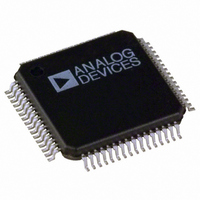
ADUC7024BSTZ62 Analog Devices Inc, ADUC7024BSTZ62 Datasheet - Page 78

ADUC7024BSTZ62
Manufacturer Part Number
ADUC7024BSTZ62
Description
IC MCU FLASH 62K ANLG I/O 64LQFP
Manufacturer
Analog Devices Inc
Series
MicroConverter® ADuC7xxxr
Specifications of ADUC7024BSTZ62
Core Size
16/32-Bit
Program Memory Size
62KB (62K x 8)
Design Resources
Sensing Low-g Acceleration Using ADXL345 Digital Accelerometer Connected to ADuC7024 (CN0133)
Core Processor
ARM7
Speed
44MHz
Connectivity
EBI/EMI, I²C, SPI, UART/USART
Peripherals
PLA, PWM, PSM, Temp Sensor, WDT
Number Of I /o
30
Program Memory Type
FLASH
Ram Size
8K x 8
Voltage - Supply (vcc/vdd)
2.7 V ~ 3.6 V
Data Converters
A/D 10x12b; D/A 2x12b
Oscillator Type
Internal
Operating Temperature
-40°C ~ 125°C
Package / Case
64-LQFP
Controller Family/series
(ARM7) ADUC
No. Of I/o's
30
Ram Memory Size
8KB
Cpu Speed
44MHz
No. Of Timers
4
Digital Ic Case Style
LQFP
Embedded Interface Type
I2C, SPI, UART
Rohs Compliant
Yes
Package
64LQFP
Device Core
ARM7TDMI
Family Name
ADuC7xxx
Maximum Speed
44 MHz
Operating Supply Voltage
3.3 V
Data Bus Width
16|32 Bit
Number Of Programmable I/os
30
Interface Type
I2C/SPI/UART
On-chip Adc
10-chx12-bit
On-chip Dac
2-chx12-bit
Number Of Timers
4
Lead Free Status / RoHS Status
Lead free / RoHS Compliant
Eeprom Size
-
Lead Free Status / RoHS Status
Lead free / RoHS Compliant, Lead free / RoHS Compliant
Available stocks
Company
Part Number
Manufacturer
Quantity
Price
Company:
Part Number:
ADUC7024BSTZ62
Manufacturer:
AD
Quantity:
261
Company:
Part Number:
ADUC7024BSTZ62
Manufacturer:
ADI
Quantity:
248
Company:
Part Number:
ADUC7024BSTZ62
Manufacturer:
Analog Devices Inc
Quantity:
10 000
Part Number:
ADUC7024BSTZ62
Manufacturer:
ADI/亚德诺
Quantity:
20 000
Company:
Part Number:
ADUC7024BSTZ62-RL
Manufacturer:
VISHAY
Quantity:
120
Company:
Part Number:
ADUC7024BSTZ62-RL
Manufacturer:
Analog Devices Inc
Quantity:
10 000
ADuC7019/20/21/22/24/25/26/27/28
Table 76. T1CON MMR Bit Descriptions
Bit
31:18
17
16:12
11:9
8
7
6
5:4
3:0
T1CLRI Register
Name
T1CLRI
T1CLRI is an 8-bit register. Writing any value to this register
clears the Timer1 interrupt.
T1CAP Register
Name
T1CAP
T1CAP is a 32-bit register. It holds the value contained in
T1VAL when a particular event occurrs. This event must be
selected in T1CON.
Timer2 (Wake-Up Timer)
Timer2 is a 32-bit wake-up timer (count-down or count-up)
with a programmable prescaler. The source can be the 32 kHz
external crystal, the core clock frequency, or the internal 32 kHz
oscillator. The clock source can be scaled by a factor of 1, 16,
256, or 32,768. The wake-up timer continues to run when the
core clock is disabled.
The counter can be formatted as plain 32-bit value or as
Hours: Minutes: Seconds: Hundredths.
Value
000
001
010
011
00
01
10
11
0000
0100
1000
1111
Address
0xFFFF032C
Address
0xFFFF0330
Description
Reserved.
Event Select Bit. Set by user to enable time
capture of an event. Cleared by user to
disable time capture of an event.
Event Select Range, 0 to 31. These events are
as described in Table 73. All events are offset
by two, that is, Event 2 in Table 73 becomes
Event 0 for the purposes of Timer1.
Clock Select.
Core Clock (HCLK).
External 32.768 kHz Crystal.
P1.0 Raising Edge Triggered.
P0.6 Raising Edge Triggered.
Count Up. Set by user for Timer1 to count up.
Cleared by user for Timer1 to count down by
default.
Timer1 Enable Bit. Set by user to enable
Timer1. Cleared by user to disable Timer1 by
default.
Timer1 Mode. Set by user to operate in
periodic mode. Cleared by user to operate in
free-running mode. Default mode.
Format.
Binary.
Reserved.
Hr: Min: Sec: Hundredths (23 hours to 0 hour).
Hr: Min: Sec: Hundredths (255 hours to 0 hour).
Prescale.
Source Clock/1.
Source Clock/16.
Source Clock/256.
Source Clock/32,768.
Default Value
0xFF
Default Value
0x00000000
Access
W
Access
R
Rev. B | Page 78 of 92
Timer2 can be used to start ADC conversions as shown in the
block diagram in Figure 66.
Timer2 interface consists of four MMRs: T2LD, T2VAL,
T2CON, and T2CLRI.
T2LD Register
Name
T2LD
T2LD is a 32-bit register load register.
T2VAL Register
Name
T2VAL
T2VAL is a 32-bit read-only register that represents the current
state of the counter.
T2CON Register
Name
T2CON
T2CON is the configuration MMR described in Table 77.
Table 77. T2CON MMR Bit Descriptions
Bit
31:11
10:9
8
7
6
5:4
3:0
OSCILLATOR
EXTERNAL
INTERNAL
CRYSTAL
HCLK
Value
00
01
10
11
00
01
10
11
0000
0100
1000
1111
Address
0xFFFF0340
Address
0xFFFF0344
Address
0xFFFF0348
Description
Reserved.
Clock Source.
External Crystal.
External Crystal.
Internal Oscillator.
Core Clock (41 MHz/2
Count Up. Set by user for Timer2 to count up.
Cleared by user for Timer2 to count down by
default.
Timer2 Enable Bit. Set by user to enable Timer2.
Cleared by user to disable Timer2 by default.
Timer2 Mode. Set by user to operate in
periodic mode. Cleared by user to operate in
free-running mode. Default mode.
Format.
Binary.
Reserved.
Hr: Min: Sec: Hundredths (23 hours to 0 hour).
Hr: Min: Sec: Hundredths (255 hours to 0 hour).
Prescale.
Source Clock/1 by Default.
Source Clock/16.
Source Clock/256 Expected for Format 2 and
Format 3.
Source Clock/32,768.
Figure 66. Timer2 Block Diagram
PRESCALER
/1, 16, 256
OR 32768
Default Value
0x00000000
Default Value
0xFFFFFFFF
Default Value
0x0000
CD
COUNTER
UP/DOWN
TIMER2
).
VALUE
32-BIT
32-BIT
LOAD
TIMER2 IRQ
Access
R/W
Access
R
Access
R/W


