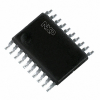
P89LPC922FDH,512 NXP Semiconductors, P89LPC922FDH,512 Datasheet - Page 7

P89LPC922FDH,512
Manufacturer Part Number
P89LPC922FDH,512
Description
IC 80C51 MCU FLASH 8K 20-TSSOP
Manufacturer
NXP Semiconductors
Series
LPC900r
Datasheet
1.P89LPC922FDH512.pdf
(46 pages)
Specifications of P89LPC922FDH,512
Core Processor
8051
Core Size
8-Bit
Speed
18MHz
Connectivity
I²C, UART/USART
Peripherals
Brown-out Detect/Reset, LED, POR, PWM, WDT
Number Of I /o
18
Program Memory Size
8KB (8K x 8)
Program Memory Type
FLASH
Ram Size
256 x 8
Voltage - Supply (vcc/vdd)
2.4 V ~ 3.6 V
Oscillator Type
Internal
Operating Temperature
-40°C ~ 85°C
Package / Case
20-TSSOP
Processor Series
P89LPC9x
Core
80C51
Data Bus Width
8 bit
Data Ram Size
256 B
Interface Type
I2C, UART
Maximum Clock Frequency
18 MHz
Number Of Programmable I/os
18
Number Of Timers
2
Operating Supply Voltage
2.4 V to 3.6 V
Maximum Operating Temperature
+ 85 C
Mounting Style
SMD/SMT
3rd Party Development Tools
PK51, CA51, A51, ULINK2
Minimum Operating Temperature
- 40 C
For Use With
622-1014 - BOARD FOR LPC9XX TSSOP622-1010 - BOARD FOR LPC922 TSSOP622-1008 - BOARD FOR LPC9103 10-HVSON622-1006 - SOCKET ADAPTER BOARDEPM900K - EMULATOR/PROGRAMMER NXP P89LPC9568-4000 - DEMO BOARD SPI/I2C TO DUAL UART568-3510 - DEMO BOARD SPI/I2C TO UART622-1002 - USB IN-CIRCUIT PROG LPC9XX568-1759 - EMULATOR DEBUGGER/PROGRMMR LPC9X
Lead Free Status / RoHS Status
Lead free / RoHS Compliant
Eeprom Size
-
Data Converters
-
Lead Free Status / Rohs Status
Details
Other names
568-2452
935273788512
P89LPC922FDH
935273788512
P89LPC922FDH
Philips Semiconductors
Table 3:
9397 750 14469
Product data
Symbol
P1.0 to P1.7
Pin description
Pin
12
11
10
9
8
4
3
2
Type
I/O, I
I/O
O
I/O
I
I/O
I/O
I/O
I/O
I
I/O
I/O
I
I
I
I/O
I/O
…continued
[1]
Description
Port 1: Port 1 is an 8-bit I/O port with a user-configurable output type, except for three
pins as noted below. During reset Port 1 latches are configured in the input only mode
with the internal pull-up disabled. The operation of the configurable Port 1 pins as inputs
and outputs depends upon the port configuration selected. Each of the configurable
port pins are programmed independently. Refer to
and
used as outputs. P1.5 is input only.
All pins have Schmitt triggered inputs.
Port 1 also provides various special functions as described below:
P1.0 — Port 1 bit 0.
TXD — Transmitter output for the serial port.
P1.1 — Port 1 bit 1.
RXD — Receiver input for the serial port.
P1.2 — Port 1 bit 2 (open-drain when used as output).
T0 — Timer/counter 0 external count input or overflow output (open-drain when used as
output).
SCL — I
P1.3 — Port 1 bit 3 (open-drain when used as output).
INT0 — External interrupt 0 input.
SDA — I
P1.4 — Port 1 bit 4. High current source (P89LPC9221).
INT1 — External interrupt 1 input.
P1.5 — Port 1 bit 5 (input only).
RST — External Reset input (if selected via FLASH configuration). A LOW on this pin
resets the microcontroller, causing I/O ports and peripherals to take on their default
states, and the processor begins execution at address 0. When using an oscillator
frequency above 12 MHz, the reset input function of P1.5 must be enabled. An
external circuit is required to hold the device in reset at power-up until V
reached its specified level. When system power is removed V
minimum specified operating voltage. When using an oscillator frequency above
12 MHz, in some applications, an external brownout detect circuit may be
required to hold the device in reset when V
operating voltage.
P1.6 — Port 1 bit 6. High current source (P89LPC9221).
P1.7 — Port 1 bit 7. High current source (P89LPC9221).
Table 8 “DC electrical characteristics”
2
2
C serial clock input/output.
C serial data input/output.
Rev. 08 — 15 December 2004
P89LPC920/921/922/9221
8-bit microcontrollers with two-clock 80C51 core
for details. P1.2 - P1.3 are open drain when
DD
falls below the minimum specified
Section 8.12.1 “Port configurations”
© Koninklijke Philips Electronics N.V. 2004. All rights reserved.
DD
will fall below the
DD
has
7 of 46


