STEVAL-ISB005V1 STMicroelectronics, STEVAL-ISB005V1 Datasheet - Page 10
STEVAL-ISB005V1
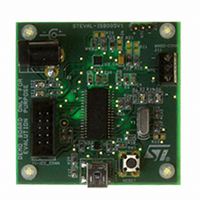
Manufacturer Part Number
STEVAL-ISB005V1
Description
BOARD EVAL CHARGER ST7260/L6924D
Manufacturer
STMicroelectronics
Type
Battery Managementr
Specifications of STEVAL-ISB005V1
Main Purpose
Power Management, Battery Charger
Embedded
Yes, MCU, 8-Bit
Utilized Ic / Part
L6924, ST72F63BK6M1
Primary Attributes
1 Cell- Li-Ion / Li-Pol, 5 V (USB Input)
Secondary Attributes
Powered by Wall Adaptor Also, LED Status Indicators
Input Voltage
5 V
Product
Power Management Modules
Lead Free Status / RoHS Status
Lead free / RoHS Compliant
For Use With/related Products
L6924D, ST7260
Other names
497-8428
Available stocks
Company
Part Number
Manufacturer
Quantity
Price
Company:

Part Number:
STEVAL-ISB005V1
Manufacturer:
STMicroelectronics
Quantity:
1


Pin description
Note:
10/139
1
2
3
4
RESET (see Note 1): Bidirectional. This active low signal forces the initialization of the MCU.
This event is the top priority non maskable interrupt. This pin is switched low when the
Watchdog is triggered or the V
OSCIN/OSCOUT: Input/Output Oscillator pin. These pins connect a parallel-resonant
crystal, or an external source, to the on-chip oscillator.
V
V
Alternate functions: Several pins of the I/O ports assume software programmable
alternate functions as shown in the pin description.
Note 1: Adding two 100 nF decoupling capacitors on the Reset pin (respectively connected
to VDD and VSS) will significantly improve product electromagnetic susceptibility
performance.
To enhance the reliability of operation, it is recommended that V
together on the application board. This also applies to V
The USBOE alternate function is mapped on Port C2 in QFN40 devices. In SO24 devices it
is mapped on Port B1.
The timer OCMP1 alternate function is mapped on Port A6 in QFN40 pin devices. In SO24
devices it is not available.
Legend / abbreviations for
Type:
In/Output level: CT = CMOS 0.3 V
Output level:
Port and control configuration:
●
●
The RESET configuration of each pin is shown in bold. This configuration is kept as long as
the device is under reset state.
DD
DDA
/V
Input:
Output:
/V
SS
SSA
(see Note 2): Main power supply and ground voltages.
(see Note 2): Power supply and ground voltages for analog peripherals.
OD = open drain, PP = push-pull, T = True open drain
I = input, O = output, S = supply
10 mA = 10 mA high sink (Fn N-buffer only)
25 mA = 25 mA very high sink (on N-buffer only)
float = floating, wpu = weak pull-up, int = interrupt
Figure
DD
is low. It can be used to reset external peripherals.
DD
2,
/ 0.7 V
Figure 3
DD
with input trigger
and
Table
SSA
2,
and V
Table
DDA
SS
3:
and V
.
DD
be connected
ST7260xx
Related parts for STEVAL-ISB005V1
Image
Part Number
Description
Manufacturer
Datasheet
Request
R

Part Number:
Description:
BOARD RGB CTR ST7,STP08C596MTR
Manufacturer:
STMicroelectronics
Datasheet:

Part Number:
Description:
Power Management IC Development Tools Full Speed USB to RS232 Bridge Demo
Manufacturer:
STMicroelectronics
Datasheet:
Part Number:
Description:
Power Management IC Development Tools 2.5W solar eval BRD USB SPV1040 LD39050
Manufacturer:
STMicroelectronics
Datasheet:

Part Number:
Description:
BOARD EVAL FOR MEMS SENSORS
Manufacturer:
STMicroelectronics
Datasheet:

Part Number:
Description:
KIT DEV STARTER ST10F276Z5
Manufacturer:
STMicroelectronics
Datasheet:

Part Number:
Description:
BOARD EVAL HDMI $ VIDEO SWITCH
Manufacturer:
STMicroelectronics
Datasheet:

Part Number:
Description:
BOARD DEMO ACCELEROMETER DIL24
Manufacturer:
STMicroelectronics
Datasheet:

Part Number:
Description:
BOARD STLM75/STDS75/ST72F651
Manufacturer:
STMicroelectronics
Datasheet:

Part Number:
Description:
EVAL BOARD 3AXIS MEMS ACCELLRMTR
Manufacturer:
STMicroelectronics
Datasheet:

Part Number:
Description:
BOARD EVAL 8BIT MICRO + TDE1708
Manufacturer:
STMicroelectronics
Datasheet:
Part Number:
Description:
STMicroelectronics [RIPPLE-CARRY BINARY COUNTER/DIVIDERS]
Manufacturer:
STMicroelectronics
Datasheet:
Part Number:
Description:
STMicroelectronics [LIQUID-CRYSTAL DISPLAY DRIVERS]
Manufacturer:
STMicroelectronics
Datasheet:
Part Number:
Description:
BOARD EVAL FOR MEMS SENSORS
Manufacturer:
STMicroelectronics
Datasheet: