STEVAL-ISB005V1 STMicroelectronics, STEVAL-ISB005V1 Datasheet
STEVAL-ISB005V1
Specifications of STEVAL-ISB005V1
Available stocks


Related parts for STEVAL-ISB005V1


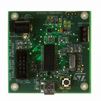
STEVAL-ISB005V1 Summary of contents
Page 1
Low speed USB 8-bit MCU family with Flash Features ■ Memories – Kbytes program memory: high density Flash (HDFlash), or FastROM with readout and write protection – In-application programming (IAP) and in- circuit programming ...
Page 2
Contents Contents 1 Description . . . . . . . . . . . . . . . . . . . . . . . . . . . . . . . . . . . . ...
Page 3
ST7260xx 7.3 Clock system . . . . . . . . . . . . . . . . . . . . . . . . . . . . . . . . . . . . ...
Page 4
Contents 12.4 16-bit timer . . . . . . . . . . . . . . . . . . . . . . . . . . . . . . . . . . . . ...
Page 5
ST7260xx 14.4.9 14.4.10 Endpoint 0 register B (EP0RB ...
Page 6
Contents 16.6.1 16.6.2 16.7 EMC characteristics . . . . . . . . . . . . . . . . . . . . . . . . . . . . . . . . . . ...
Page 7
ST7260xx 1 Description The ST7260xx devices are members of the ST7 microcontroller family designed for USB applications running from 4.0 to 5.5 V. Different package options offer I/O pins. All devices are based on a common industry-standard ...
Page 8
Block diagram 2 Block diagram Figure 1. General block diagram OSCIN OSCOUT RESET V /TEST PP V DDA V SSA MHz OSCIN frequency required to generate 6 MHz USB clock. 8/139 INTERNAL ...
Page 9
ST7260xx 3 Pin description Figure 2. 40-lead QFN package pinout Note: NC=Do not connect Figure 3. 24-pin SO package pinout PA0/MCO SSA USBDP 3 USBDM 4 USBV ...
Page 10
Pin description RESET (see Note 1): Bidirectional. This active low signal forces the initialization of the MCU. This event is the top priority non maskable interrupt. This pin is switched low when the Watchdog is triggered or the V OSCIN/OSCOUT: ...
Page 11
ST7260xx ) Table 2. Device pin description (QFN40) Pin n° Pin name 1 PA0/MCO 2 V SSA 3 USBDP 4 USBDM 5 USBVCC 6 V DDA OSCOUT 9 OSCIN PC2/USBOE 12 PC1/TDO ...
Page 12
Pin description Table 2. Device pin description (QFN40) (continued) Pin n° Pin name 30 PA3/EXTCLK 31 PA2/ICCCLK PA1/ICCDATA 12/139 Level Port / control ...
Page 13
ST7260xx Table 3. Device pin description (SO24) Pin n° Pin name OSCOUT 3 OSCIN PC1/TDO 6 PC0/RDI 7 RESET 8 PB6/IT7 9 V /TEST PP 10 PB3 11 PB2 12 PB1/USBOE 13 ...
Page 14
Register & memory map 4 Register & memory map As shown in Figure registers. The available memory locations consist 384 bytes of RAM including 64 bytes of register locations, and Kbytes of user program ...
Page 15
ST7260xx . Table 4. Interrupt vector map Vector address FFE0h-FFEDh FFEEh-FFEFh USB interrupt vector FFF0h-FFF1h SCI interrupt vector FFF2h-FFF3h TIMER interrupt vector FFF4h-FFF5h IT1 to IT8 interrupt vector FFF6h-FFF7h USB end suspend mode interrupt vector FFF8h-FFF9h Flash start programming interrupt ...
Page 16
Register & memory map Table 5. Hardware register memory map (continued) Address Block Register label 0011h TCR2 0012h TCR1 0013h TCSR 0014h TIC1HR 0015h TIC1LR 0016h TOC1HR 0017h TOC1LR 0018h TIM TCHR 0019h TCLR 001Ah TACHR 001Bh TACLR 001Ch TIC2HR ...
Page 17
ST7260xx 5 Flash program memory 5.1 Introduction The ST7 dual voltage High Density Flash (HDFlash non-volatile memory that can be electrically erased as a single block or by individual sectors and programmed on a byte-by- byte basis using ...
Page 18
Flash program memory 5.3.1 Readout protection Readout protection, when selected, provides a protection against program memory content extraction and against write access to Flash memory. Even if no protection can be considered as totally unbreakable, the feature provides a very ...
Page 19
ST7260xx 5.4 ICC interface ICC needs a minimum of 4 and pins to be connected to the programming tool (see Figure 6). These pins are: – RESET: device reset – device power supply ground SS ...
Page 20
... Depending on the ICP code downloaded in RAM, Flash memory programming can be fully customized (number of bytes to program, program locations, or selection serial communication interface for downloading). When using an STMicroelectronics or third-party programming tool that supports ICP and the specific microcontroller device, the user needs only to implement the ICP hardware interface on the application board (see to the device pinout description ...
Page 21
ST7260xx 6 Central processing unit (CPU) 6.1 Introduction This CPU has a full 8-bit architecture and contains six internal registers allowing efficient 8- bit data manipulation. 6.2 Main features ● 63 basic instructions ● Fast 8-bit by 8-bit multiply ● ...
Page 22
Central processing unit (CPU) 6.3.1 Accumulator (A) The Accumulator is an 8-bit general purpose register used to hold operands and the results of the arithmetic and logic calculations and to manipulate data. 6.3.2 Index registers (X and Y) In indexed ...
Page 23
ST7260xx Table 8. CC register description BIt Name Interrupt mask This bit is set by hardware when entering in interrupt or by software to disable all interrupts except the TRAP software interrupt. This bit is cleared by software. 0: Interrupts ...
Page 24
Central processing unit (CPU) 6.3.5 Stack pointer register (SP The Stack Pointer is a 16-bit register which is always pointing to the next free location in the stack then decremented after ...
Page 25
ST7260xx 7 Reset and clock management 7.1 Reset The Reset procedure is used to provide an orderly software start- exit low power modes. Three reset modes are provided: a low voltage (LVD) reset, a watchdog reset and an ...
Page 26
Reset and clock management Figure 9. Low voltage detector functional diagram V DD Figure 10. Low voltage reset signal output V DD RESET Note: Hysteresis (V -V IT+ Figure 11. Temporization timing diagram after an internal reset V DD Addresses ...
Page 27
ST7260xx Figure 12. Reset timing diagram t DDR V DD OSCIN f CPU PC RESET WATCHDOG RESET Note: Refer to Electrical Characteristics for values of t 7.3 Clock system 7.3.1 General description The MCU accepts either a crystal or ceramic ...
Page 28
Reset and clock management Table 9. Recommended values for 24 MHz crystal resonator Symbol (1) R SMAX C OSCIN C OSCOUT the equivalent serial resistor of the crystal (see crystal specification). SMAX 7.3.2 External clock ...
Page 29
ST7260xx Figure 15. Clock block diagram MHz 0 CPU and peripherals SMS 1 6 MHz (USB MHz %2 Crystal OSC24/12 Reset and clock management 29/139 ...
Page 30
Interrupts 8 Interrupts The ST7 core may be interrupted by one of two different methods: maskable hardware interrupts as listed in (TRAP). The Interrupt processing flowchart is shown in The maskable interrupts must be enabled clearing the I bit in ...
Page 31
ST7260xx Peripheral interrupts Different peripheral interrupt flags in the status register are able to cause an interrupt when they are active if both: ● The I bit of the CC register is cleared. ● The corresponding enable bit is set ...
Page 32
Interrupts Table 10. Interrupt mapping Source N° block RESET TRAP FLASH Flash Start Programming Interrupt USB 1 ITi 2 TIMER Timer Peripheral Interrupts 3 4 SCI SCI Peripheral Interrupts 5 USB USB Peripheral Interrupts 8.0.1 Interrupt register (ITRFRE) ITRFRE 7 ...
Page 33
ST7260xx 9 Power saving modes 9.1 Introduction To give a large measure of flexibility to the application in terms of power consumption, two main power saving modes are implemented in the ST7. After a RESET, the normal operating mode is ...
Page 34
Power saving modes Figure 17. Halt mode flowchart Note: Before servicing an interrupt, the CC register is pushed on the stack. The I-Bit is set during the interrupt routine and cleared when the CC register is popped. 9.3 Slow mode ...
Page 35
ST7260xx The MCU will remain in Wait mode until a Reset or an Interrupt occurs, causing it to wake up. Refer to Figure 18. Related documentation ● AN 980: ST7 keypad decoding techniques, implementing wake-up on keystroke ● AN1014: How ...
Page 36
I/O ports 10 I/O ports 10.1 Introduction The I/O ports offer different functional modes: ● Transfer of data through digital inputs and outputs and for specific pins ● Alternate signal input/output for the on-chip peripherals ● External interrupt generation An ...
Page 37
ST7260xx In this mode, writing “0” or “1” to the DR register applies this digital value to the I/O pin through the latch. Therefore, the previously saved value is restored when the DR register is read. Note: The interrupt function ...
Page 38
I/O ports Figure 19. PA0, PA3, PA4, PA5, PA6, PA7 configuration DDR SEL DR SEL ALTERNATE INPUT Table 15. PA1, PA2 description Port A PA1 without pull-up PA2 without pull-up 1. Reset state 38/139 ALTERNATE ENABLE 1 ALTERNATE OUTPUT 0 ...
Page 39
ST7260xx Figure 20. PA1, PA2 configuration 10.2.2 Port B Table 16. Port B description Port B PB0 without pull-up PB1 without pull-up PB2 without pull-up PB3 without pull-up PB4 without pull-up PB5 without pull-up PB6 without pull-up ALTERNATE ENABLE 1 ...
Page 40
I/O ports Table 16. Port B description (continued) Port B PB7 without pull-up 1. Reset state 2. On SO24 only Figure 21. Port B configuration LATCH LATCH DDR SEL DR SEL ALTERNATE INPUT 10.2.3 Port C Table 17. Port C ...
Page 41
ST7260xx Figure 22. Port C configuration DR LATCH DDR LATCH DDR SEL DR SEL ALTERNATE INPUT 10.2.4 Register description 10.2.5 Data register (PxDR) PADR PBDR PCDR R/W R/W Table 18. PxDR register description Bit Name Data ...
Page 42
I/O ports 10.2.6 Data direction register (PxDDR) PADDR PBDDR PCDDR 7 6 DD7 DD6 R/W R/W Table 19. PxDDR register description Bit Name Data Direction bits The DDR register gives the input/output direction configuration of the pins. Each bit is ...
Page 43
ST7260xx 11 Miscellaneous register MISCR Table 21. MISCR register description Bit Name 7:3 Reserved Slow mode select This bit is set by software and only cleared by hardware after a reset. If this bit is set, ...
Page 44
Watchdog timer (WDG) 12 Watchdog timer (WDG) 12.1 Introduction The Watchdog timer is used to detect the occurrence of a software fault, usually generated by external interference or by unforeseen logical conditions, which causes the application program to abandon its ...
Page 45
ST7260xx Figure 23. Watchdog block diagram f CPU Table 23. Watchdog timing (f Max Min Note: 1 Following a reset, the watchdog is disabled. Once activated it cannot be disabled, except by a reset. 2 The T6 bit can be ...
Page 46
Watchdog timer (WDG) 12.3.3 Low power modes WAIT Instruction No effect on Watchdog. HALT Instruction If the Watchdog reset on HALT option is selected by option byte, a HALT instruction causes an immediate reset generation if the Watchdog is activated ...
Page 47
ST7260xx 12.3.6 Control register (WDGCR) WDGCR 7 6 WDGA R/W Table 24. WDGCR register description Bit Name Activation bit This bit is set by software and only cleared by hardware after a reset. When WDGA = 1, the watchdog can ...
Page 48
Watchdog timer (WDG) 12.4 16-bit timer 12.4.1 Introduction The timer consists of a 16-bit free-running counter driven by a programmable prescaler. It may be used for a variety of purposes, including pulse length measurement two input signals ...
Page 49
ST7260xx 12.4.3 Functional description Counter The main block of the programmable timer is a 16-bit free running upcounter and its associated 16-bit registers. The 16-bit registers are made up of two 8-bit registers called high and low. ● Counter Register ...
Page 50
Watchdog timer (WDG) Figure 24. Timer block diagram fCPU EXEDG 1/2 1/4 1/8 EXTCLK pin CC[1:0] ICF1 OCF1 TOF ICIE OCIE TOIE (See note 1) Timer interrupt 1. If IC, OC and TO interrupt requests have separate vectors then the ...
Page 51
ST7260xx 16-bit read sequence The 16-bit read sequence (from either the Counter register or the Alternate Counter register) is illustrated in the following 16-bit read sequence Figure 25. The user must first read the MSB, afterwhich the LSB value is ...
Page 52
Watchdog timer (WDG) External clock The external clock (where available) is selected if CC0 = 1 and CC1 = 1 in the CR2 register. The status of the EXEDG bit in the CR2 register determines the type of level transition ...
Page 53
ST7260xx Input capture In this section, the index, i, may because there are two input capture functions in the 16-bit timer. The two 16-bit input capture registers (IC1R/IC2R) are used to latch the value of the ...
Page 54
Watchdog timer (WDG) Note: 1 After reading the ICiHR register, transfer of input capture data is inhibited and ICFi will never be set until the ICiLR register is also read. 2 The ICiR register contains the free running counter value ...
Page 55
ST7260xx Output compare In this section, the index, i, may because there are two output compare functions in the 16-bit timer. This function can be used to control an output waveform or indicate when a period ...
Page 56
Watchdog timer (WDG) If the timer clock is an external clock, the formula is: Where: Δt = Output compare period (in seconds External timer clock frequency (in hertz) EXT Clearing the output compare interrupt request (that is, clearing ...
Page 57
ST7260xx Figure 31. Output compare block diagram 16-bit free running counter 16-bit Output compare 16-bit 16-bit OC1R register OC2R register Figure 32. Output compare timing diagram, f Output Compare register i (OCRi) Figure 33. Output compare timing diagram, f Output ...
Page 58
Watchdog timer (WDG) One pulse mode One Pulse mode enables the generation of a pulse when an external event occurs. This mode is selected via the OPM bit in the CR2 register. The one pulse mode uses the Input Capture1 ...
Page 59
ST7260xx The OC1R register value required for a specific timing application can be calculated using the following formula: Where Pulse period (in seconds CPU clock frequnency (in hertz) CPU PRESC = Timer prescaler factor (2, 4 ...
Page 60
Watchdog timer (WDG) Figure 36. Pulse width modulation mode timing example with two output compare functions Counter 34E2 OCMP1 1. OC1R = 2ED0h, OC2R = 34E2, OLVL1 = 0, OLVL2 = timers with only one Output Compare ...
Page 61
ST7260xx Figure 37. Pulse width modulation cycle If OLVL1 = 1 and OLVL2 = 0, the length of the positive pulse is the difference between the OC2R and OC1R registers. If OLVL1 = OLVL2, a continuous signal will be seen ...
Page 62
Watchdog timer (WDG) 12.4.4 Low power modes Table 28. Effect of low power modes on 16-bit timer Mode No effect on 16-bit timer. Wait Timer interrupts cause the device to exit from Wait mode. 16-bit timer registers are frozen. In ...
Page 63
ST7260xx 12.4.6 Summary of timer modes Table 30. Summary of timer modes Mode Input Capture (1 and/or 2) Output Compare (1 and/or 2) One Pulse mode PWM mode 1. See note 4 in One pulse mode on page 2. See ...
Page 64
Watchdog timer (WDG) Table 31. CR1 register description (continued) Bit Name Forced Output compare 2 This bit is set and cleared by software. 4 FOLV2 0: No effect on the OCMP2 pin. 1: Forces the OLVL2 bit to be copied ...
Page 65
ST7260xx Table 32. CR2 register description (continued) Bit Name One Pulse Mode 0: One Pulse mode is not active. 5 OPM 1: One Pulse mode is active, the ICAP1 pin can be used to trigger one pulse on the OCMP1 ...
Page 66
Watchdog timer (WDG) Table 33. CSR register description (continued) Bit Name Output Compare Flag match (reset value). 6 OCF1 1: The content of the free running counter has matched the content of the OC1R register. To clear ...
Page 67
ST7260xx Input capture 1 low register (IC1LR) This is an 8-bit register that contains the low part of the counter value (transferred by the input capture 1 event). IC1LR 7 6 MSB RO RO Output compare 1 high register (OC1HR) ...
Page 68
Watchdog timer (WDG) Output compare 2 low register (OC2LR) This is an 8-bit register that contains the low part of the value to be compared to the CLR register. OC2LR 7 6 MSB R/W R/W Counter high register (CHR) This ...
Page 69
ST7260xx Alternate counter low register (ACLR) This is an 8-bit register that contains the low part of the counter value. A write to this register resets the counter. An access to this register after an access to CSR register does ...
Page 70
Watchdog timer (WDG) Table 34. 16-bit timer register map and reset values Address Register (Hex.) label CR1 11 Reset value CR2 12 Reset value CSR 13 Reset value IC1HR 14 Reset value IC1LR 15 Reset value OC1HR 16 Reset value ...
Page 71
ST7260xx 13 Serial communications interface (SCI) 13.1 Introduction The Serial Communications Interface (SCI) offers a flexible means of full-duplex data exchange with external equipment requiring an industry standard NRZ asynchronous serial data format. The SCI offers a very wide range ...
Page 72
Serial communications interface (SCI) 13.2.1 General description The interface is externally connected to another device by two pins (see ● TDO: Transmit Data Output. When the transmitter and the receiver are disabled, the output pin returns to its I/O port ...
Page 73
ST7260xx Figure 38. SCI block diagram TDO RDI CR2 TIE TCIE INTERRUPT CONTROL TRANSMITTER CLOCK f CPU 13.2.2 Functional description The block diagram of the Serial Control Interface, is shown in dedicated registers: ● Two control registers (SCICR1 & SCICR2) ...
Page 74
Serial communications interface (SCI) Serial data format Word length may be selected as being either bits by programming the M bit in the SCICR1 register (see The TDO pin is in low state during the start bit. ...
Page 75
ST7260xx Procedure ● Select the M bit to define the word length. ● Select the desired baud rate using the SCIBRR and the SCIETPR registers. ● Set the TE bit to assign the TDO pin to the alternate function and ...
Page 76
Serial communications interface (SCI) Note: Resetting and setting the TE bit causes the data in the TDR register to be lost. Therefore the best time to toggle the TE bit is when the TDRE bit is set i.e. before writing ...
Page 77
ST7260xx Noise error Oversampling techniques are used for data recovery by discriminating between valid incoming data and noise. Normal data bits are considered valid if three consecutive samples (8th, 9th, 10th) have the same bit value, otherwise the NF flag ...
Page 78
Serial communications interface (SCI) Baud rate generation The baud rate for the receiver and transmitter (Rx and Tx) are set independently and calculated as follows: f CPU Tx = (16 PR with ...
Page 79
ST7260xx Parity control Parity control (generation of parity bit in transmission and parity checking in reception) can be enabled by setting the PCE bit in the SCICR1 register. Depending on the frame length defined by the M bit, the possible ...
Page 80
Serial communications interface (SCI) clock occurs just before the pin value changes, the samples would then be out of sync by ~4 µs. This means the entire bit length must be at least 40 µs (36µs for the 10th sample ...
Page 81
ST7260xx Figure 40. Bit sampling in reception mode RDI LINE Sample clock 13.2.3 Low power modes Table 36. Effect of low power modes on SCI Mode No effect on SCI. Wait SCI interrupts cause the device to exit from Wait ...
Page 82
Serial communications interface (SCI) 13.3 Register description 13.3.1 Status register (SCISR) SCISR 7 6 TDRE Table 38. SCISR register description Bit Name Transmit Data Register Empty This bit is set by hardware when the content of the ...
Page 83
ST7260xx Table 38. SCISR register description (continued) Bit Name Overrun error This bit is set by hardware when the word currently being received in the shift register is ready to be transferred into the RDR register while RDRF = 1. ...
Page 84
Serial communications interface (SCI) 13.3.2 Control register 1 (SCICR1) SCICR1 R/W R/W Table 39. SCICR1 register description Bit Name Receive data bit This bit is used to store the 9th bit of the ...
Page 85
ST7260xx Table 39. SCICR1 register description (continued) Bit Name Parity Selection This bit selects the odd or even parity when the parity generation/detection is enabled (PCE bit set set and cleared by software. The parity will be selected ...
Page 86
Serial communications interface (SCI) Table 40. SCICR2 register description (continued) Bit Name Transmitter Enable This bit enables the transmitter set and cleared by software. 0: Transmitter is disabled 1: Transmitter is enabled Notes During transmission, ...
Page 87
ST7260xx 13.3.5 Baud rate register (SCIBRR) SCIBRR 7 6 SCP[1:0] R/W Table 41. SCIBRR register description Bit Name First SCI Prescaler 7:6 SCP[1:0] SCI Transmitter rate divisor 5:3 SCT[2:0] SCI Receiver rate divisor 2:0 SCR[2:0] Table 42. SCI register map ...
Page 88
Serial communications interface (SCI) Table 42. SCI register map and reset values Address Register (Hex.) Label SCIBRR 22 Reset Value SCICR1 23 Reset Value SCICR2 24 Reset Value 88/139 SCP1 SCP0 SCT2 SCT1 ...
Page 89
ST7260xx 14 USB interface (USB) 14.1 Introduction The USB Interface implements a low-speed function interface between the USB and the ST7 microcontroller highly integrated circuit which includes the transceiver, 3.3 voltage regulator, SIE and DMA. No external ...
Page 90
USB interface (USB) Figure 41. USB block diagram USBDM USBDP USBVCC USBGND 14.4 Register description 14.4.1 DMA address register (DMAR) DMAR 7 6 DA15 DA14 R/W R/W Bits 7:0=DA[15:8] DMA address bits 15-8. Software must write the start address of ...
Page 91
ST7260xx When a CTR interrupt occurs (see register ISTR) the software should read the EP bits to identify the endpoint which has sent or received a packet. Bits 3:0 = CNT[3:0] Byte count (read only). This field shows how many ...
Page 92
USB interface (USB) Bit 2 = RX_SEZ Received single-ended zero This bit indicates the status of the RX_SEZ transceiver output SE0 (single-ended zero) state 1: USB lines are in SE0 (single-ended zero) state Bit 1 = RXD Received ...
Page 93
ST7260xx 0: No error detected 1: Timeout, CRC, bit stuffing or nonstandard framing error detected Bit 3 = IOVR Interrupt overrun. This bit is set when hardware tries to set ERR, or SOF before they have been cleared by software. ...
Page 94
USB interface (USB) 14.4.6 Control register (CTLR) CTLR R/W R/W Bits 7:4 = Reserved. Forced by hardware to 0. Bit 3 = RESUME Resume. This bit is set by software to wake-up the Host when the ...
Page 95
ST7260xx 14.4.7 Device address register (DADDR) DADDR ADD6 R/W R/W Bit 7 = Reserved. Forced by hardware to 0. Bits 6:0 = ADD[6:0] Device address, 7 bits. Software must write into this register the address sent by ...
Page 96
USB interface (USB) Table 44. STAT_TX bits STAT_TX1 These bits are written by software. Hardware sets the STAT_TX bits to NAK when a correct transfer has occurred (CTR=1) related SETUP transaction addressed ...
Page 97
ST7260xx Table 45. STAT_RX bits STAT_RX1 These bits are written by software. Hardware sets the STAT_RX bits to NAK when a correct transfer has occurred (CTR=1) related to an OUT or SETUP transaction addressed to this ...
Page 98
USB interface (USB) 1. Initialize the DMAR, IDR, and IMR registers (choice of enabled interrupts, address of DMA buffers). Refer the paragraph titled initializing the DMA Buffers. 2. Initialize the EP0RA and EP0RB registers to enable accesses to address 0 ...
Page 99
ST7260xx End suspend (ESUSP) The CPU is alerted by activity on the USB, which causes an ESUSP interrupt. The ST7 automatically terminates HALT mode. Correct transfer (CTR) 1. When this event occurs, the hardware automatically sets the STAT_TX or STAT_RX ...
Page 100
USB interface (USB) Table 46. USB register map and reset values (continued) Address Register 7 name (Hex.) EP1RA ST_OUT 2E Reset Value 0 EP1RB CTRL 2F Reset Value 0 EP2RA ST_OUT 30 Reset Value 0 EP2RB CTRL 31 Reset Value ...
Page 101
ST7260xx 15 Instruction set 15.1 ST7 addressing modes The ST7 Core features 17 different addressing modes which can be classified in 7 main groups: Table 47. Addressing mode groups Addressing mode Inherent Immediate Direct Indexed Indirect Relative Bit operation The ...
Page 102
Instruction set Table 48. ST7 addressing mode overview (continued) Mode Short Indirect Indexed ld A,([$10],X) Long Indirect Indexed ld A,([$10.w],X) Relative Direct jrne loop Relative Indirect jrne [$10] Bit Direct bset $10,#7 Bit Indirect bset [$10],#7 Bit Direct Relative btjt ...
Page 103
ST7260xx Table 49. Inherent instructions Instruction SLL, SRL, SRA, RLC, RRC SWAP 15.1.2 Immediate Immediate instructions have two bytes, the first byte contains the opcode, the second byte contains the operand value. Table 50. Immediate instructions Instruction LD CP BCP ...
Page 104
Instruction set Indexed (long) The offset is a word, thus allowing 64 Kbyte addressing space and requires 2 bytes after the opcode. 15.1.5 Indirect (short, long) The required data byte to do the operation is found by its memory address, ...
Page 105
ST7260xx Table 51. Instructions supporting direct, indexed, indirect and indirect indexed addressing modes Long and short instructions Short instructions only 15.1.7 Relative mode (direct, indirect) This addressing mode is used to modify the PC register value by adding an 8-bit ...
Page 106
Instruction set Table 53. Instruction groups Group Load and Transfer Stack operation Increment/Decrement Compare and Tests Logical operations Bit Operation Conditional Bit Test and Branch Arithmetic operations Shift and Rotates Unconditional Jump or Call Conditional Branch Interruption management Condition Code ...
Page 107
ST7260xx Table 54. Instruction set Mnemo Description ADC Add with Carry ADD Addition AND Logical And BCP Bit compare A, Memory BRES Bit Reset BSET Bit Set BTJF Jump if bit is false (0) BTJT Jump if bit is true ...
Page 108
Instruction set Table 54. Instruction set (continued) Mnemo Description JRUGT Jump JRULE Jump Load MUL Multiply NEG Negate (2's compl) NOP No Operation OR OR operation POP ...
Page 109
ST7260xx 16 Electrical characteristics 16.1 Parameter conditions Unless otherwise specified, all voltages are referred to V 16.1.1 Minimum and maximum values Unless otherwise specified the minimum and maximum values are guaranteed in the worst conditions of ambient temperature, supply voltage ...
Page 110
Electrical characteristics Figure 44. Pin input voltage 110/139 ST7 PIN V IN ST7260xx ...
Page 111
ST7260xx 16.2 Absolute maximum ratings Stresses above those listed as “absolute maximum ratings” may cause permanent damage to the device. This is a stress rating only and functional operation of the device under these conditions is not implied. Exposure to ...
Page 112
Electrical characteristics Table 57. Thermal characteristics Symbol T STG T J 16.3 Operating conditions 16.3.1 General operating conditions Table 58. General operating condition Symbol V Operating supply voltage DD V Analog supply voltage DDA V Analog supply voltage SSA f ...
Page 113
ST7260xx 16.3.2 Operating conditions with low voltage detector (LVD) Subject to general operating conditions for V Table 59. Operating conditions at power-up/power-down Symbol Low Voltage Reset Threshold V IT+ (V rising) DD Low Voltage Reset Threshold V IT- (V falling) ...
Page 114
Electrical characteristics Figure 46. Typ. I MHz f Idd Run (mA) at fcpu=4 and 8MHz 4.2 4.4 16.5 Clock and timing characteristics Subject to general operating conditions for V 16.5.1 General timings ...
Page 115
ST7260xx Table 62. Control timings (continued) Symbol Parameter t Watchdog time-out DOG Crystal oscillator t OXOV start-up time t Power up rise time DDR 1. Not tested in production, guaranteed by characterization. Conditions Min 49152 MHz 6.144 ...
Page 116
Electrical characteristics 16.5.3 External clock source Table 63. External clock characteristics Symbol OSCIN input pin high level V OSCINH voltage OSCIN input pin low level V OSCINL voltage t w(OSCINH) OSCIN high or low time t w(OSCINL) t r(OSCIN) OSCIN ...
Page 117
ST7260xx 16.6 Memory characteristics Subject to general operating conditions for f 16.6.1 RAM and hardware registers Table 64. RAM and hardware registers Symbol V Data retention mode RM 1. Guaranteed by design. Not tested in production. 16.6.2 Flash memory Operating ...
Page 118
Electrical characteristics 16.7 EMC characteristics Susceptibility and emission tests are performed on a sample basis during product characterization. 16.7.1 Functional EMS (electromagnetic susceptibility) Based on a simple running application on the product (toggling 2 LEDs through I/O ports), the product ...
Page 119
ST7260xx Table 66. EMS data Symbol Voltage limits to be applied on any I/O pin V FESD to induce a functional disturbance Fast transient voltage burst limits applied through 100pF on V FFTB pins to induce a ...
Page 120
Electrical characteristics Static latch-up Two complementary static tests are required on six parts to assess the latch-up performance. ● A supply overvoltage (applied to each power supply pin) and ● A current injection (applied to each input, output and configurable ...
Page 121
ST7260xx 16.8 I/O port pin characteristics 16.8.1 General characteristics Subject to general operating conditions for V Table 70. I/O port characteristics Symbol Parameter V Input low level voltage IL V Input high level voltage IH V Input voltage IN Schmitt ...
Page 122
Electrical characteristics Figure 52. Typ. I Figure 53. Typ. R 122/139 vs Pull-up current (µ 4.2 4.4 4.6 4.8 Vdd (V) vs Rpu ...
Page 123
ST7260xx 16.8.2 Output driving current Subject to general operating condition for V Table 71. Output current characteristics Symbol Output low level voltage for a standard I/O pin when pins are sunk at the same time, Port A0, ...
Page 124
Electrical characteristics Figure 58 130 125 120 115 110 105 4 4.2 4.4 Figure 60 current) |Vdd - Voh| (V) at Vdd=5V 0.3 0.25 0.2 0.15 0.1 0. 1.5 Figure 62 current) ...
Page 125
ST7260xx 16.9 Control pin characteristics 16.9.1 Asynchronous RESET pin Subject to general operating conditions for V Table 72. RESET pin characteristics Symbol Parameter V Input high level voltage IH V Input low voltage IL V Schmitt trigger voltage hysteresis hys ...
Page 126
Electrical characteristics RESET pin protection when LVD is enabled When the LVD is enabled recommended to protect the RESET pin as shown in Figure 64 and follow these guidelines: 1. The reset network protects the device against parasitic ...
Page 127
ST7260xx RESET pin protection when LVD is disabled When the LVD is disabled recommended to protect the RESET pin as shown in Figure 65 and follow these guidelines: 1. The reset network protects the device against parasitic resets. ...
Page 128
Electrical characteristics Figure 66. USB: data signal rise and fall time Differential Data Lines VCRS V SS Table 74. USB: low-speed electrical characteristics Symbol rfm V CRS 1. For more detailed information, please refer to ...
Page 129
ST7260xx 17 Package characteristics In order to meet environmental requirements, ST offers these devices in different grades of ® ECOPACK packages, depending on their level of environmental compliance. ECOPACK specifications, grade definitions and product status are available at: www.st.com. ® ...
Page 130
Package characteristics 17.1.1 Thermal characteristics Table 76. Package thermal characteristics Symbol R thJA Jmax 1. The maximum power dissipation is obtained from the formula application can be defined by the user with the formula: ...
Page 131
ST7260xx 18 Device configuration and ordering information Each device is available for production in user programmable versions (High Density FLASH) as well as in factory coded versions (FASTROM). ST72P60 devices are Factory Advanced Service Technique ROM (FASTROM) versions: they are ...
Page 132
... ST72P60K2U1/xxx ST72P60E2M1/xxx ST72P60K1U1/xxx ST72P60E1M1/xxx 1. /xxx stands for the ROM code name assigned by STMicroelectronics. Contact ST sales office for product availablity of FASTROM types (shaded in table). 18.3 Development tools STMicroelectronics offers a range of hardware and software development tools for the ST7 microcontroller family. Full details of tools available for the ST7 from third party manufacturers can be obtain from the STMicroelectronics Internet site: ➟ ...
Page 133
... STMicroelectronics tools features ST7 Emulator ST7 Programming Board 1. In-Circuit Programming (ICP) interface for FLASH devices. Table 80. Dedicated STMicroelectronics development tools Supported products ST7260 1. Add Suffix /EU or /US for the power supply for your region. Device configuration and ordering information Programming In-Circuit Emulation ...
Page 134
... FASTROM code must be sent in .S19 format. Hex extension cannot be processed. STMicroelectronics references: Device Type/Memory Size/Package (check only one option): ------------------------------------------------------------------------------------ ...
Page 135
ST7260xx 19 Known limitations 19.1 PA2 limitation with OCMP1 enabled Description This limitation affects only Rev B Flash devices (with Internal Sales Type 72F60xxxxx$x7); it has been corrected in Rev W Flash devices (with Internal Sales Type 72F60xxxxx$x9). Refer to ...
Page 136
Known limitations The exact sequence is: ● Disable interrupts ● Reset and Set TE (IDLE request) ● Set and Reset SBK (Break Request) ● Re-enable interrupts 136/139 ST7260xx ...
Page 137
ST7260xx 20 Device marking The silicon revision can be identified either by Rev letter or obtained via a trace code. Follow the procedure below: 1. Identify the silicon revision letter from either the device package or the box label. For ...
Page 138
Revision history 21 Revision history Table 81. Document revision history Date 13-Feb-2006 18-Oct-2006 05-Feb-2009 138/139 Revision 1 Initial release. 2 Added known limitations section Added caution in Section 7.1 on page 25 Added reference to watchdog reset pulse t page ...
Page 139
... ST7260xx Information in this document is provided solely in connection with ST products. STMicroelectronics NV and its subsidiaries (“ST”) reserve the right to make changes, corrections, modifications or improvements, to this document, and the products and services described herein at any time, without notice. All ST products are sold pursuant to ST’s terms and conditions of sale. ...