MA240017 Microchip Technology, MA240017 Datasheet - Page 188
MA240017
Manufacturer Part Number
MA240017
Description
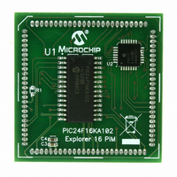
MODULE PLUG-IN PIC24F16KA102 PIM
Manufacturer
Microchip Technology
Series
PIC®r
Specifications of MA240017
Accessory Type
Plug-In Module (PIM) - PIC24F16KA102
Product
Microcontroller Modules
Data Bus Width
16 bit
Core Processor
PIC24F16KA102
Operating Supply Voltage
3 V to 3.6 V
Development Tools By Supplier
Integrated Development Environment, Assembler, ANSI C Compiler
Processor Series
PIC24F
Silicon Manufacturer
Microchip
Core Architecture
PIC
Core Sub-architecture
PIC24
Silicon Core Number
PIC24F
Silicon Family Name
PIC24FxxKAxx
Lead Free Status / RoHS Status
Lead free / RoHS Compliant
For Use With/related Products
Explorer 16 (DM240001 or DM240002)
For Use With
DM240001 - BOARD DEMO PIC24/DSPIC33/PIC32
Lead Free Status / Rohs Status
Lead free / RoHS Compliant
Available stocks
Company
Part Number
Manufacturer
Quantity
Price
Company:

Part Number:
MA240017
Manufacturer:
MICROCHIP
Quantity:
12 000


PIC24F16KA102 FAMILY
25.2
Time measurements on the pulse width can be similarly
performed using the A/D module’s internal capacitor
(C
Figure 25-2 displays the external connections used for
time measurements, and how the CTMU and A/D
modules are related in this application. This example
also shows both edge events coming from the external
CTEDG pins, but other configurations using internal
edge sources are possible.
25.3
The CTMU module can also generate an output pulse
with edges that are not synchronous with the device’s
system clock. More specifically, it can generate a pulse
with a programmable delay from an edge event input to
the module.
FIGURE 25-2:
FIGURE 25-3:
DS39927B-page 186
AD
) and a precision resistor for current calibration.
Measuring Time
Pulse Generation and Delay
TYPICAL CONNECTIONS AND INTERNAL CONFIGURATION FOR TIME
MEASUREMENT
TYPICAL CONNECTIONS AND INTERNAL CONFIGURATION FOR PULSE
DELAY GENERATION
CTEDG1
C
C2INB
DELAY
CTEDG1
CTEDG2
ANx
R
PR
EDG1
Preliminary
CV
Current Source
PIC24F Device
REF
Comparator
-
CTMU
C2
EDG2
EDG1
When the module is configured for pulse generation
delay by setting the TGEN bit (CTMUCON<12>), the
internal current source is connected to the B input of
Comparator 2. A capacitor (C
the Comparator 2 pin, C2INB, and the comparator
voltage reference, CV
CV
module begins to charge C
is detected. When C
trip point, a pulse is output on CTPLS. The length of the
pulse delay is determined by the value of C
the CV
Figure 25-3 shows the external connections for pulse
generation, as well as the relationship of the different
analog modules required. While CTEDG1 is shown as
the input pulse source, other options are available. A
detailed discussion on pulse generation with the CTMU
module is provided in the “PIC24F Family Reference
Manual”.
C
PIC24F Device
A/D Converter
AD
REF
Current Source
CTMU
REF
is then configured for a specific trip point. The
Output Pulse
trip point.
DELAY
CTPLS
REF
© 2009 Microchip Technology Inc.
, is connected to C2INA.
DELAY
charges above the CV
DELAY
when an edge event
) is connected to
DELAY
and
REF
Related parts for MA240017
Image
Part Number
Description
Manufacturer
Datasheet
Request
R

Part Number:
Description:
Manufacturer:
Microchip Technology Inc.
Datasheet:
Part Number:
Description:
Manufacturer:
Microchip Technology Inc.
Datasheet:
Part Number:
Description:
Manufacturer:
Microchip Technology Inc.
Datasheet:
Part Number:
Description:
Manufacturer:
Microchip Technology Inc.
Datasheet:
Part Number:
Description:
Manufacturer:
Microchip Technology Inc.
Datasheet:
Part Number:
Description:
Manufacturer:
Microchip Technology Inc.
Datasheet:
Part Number:
Description:
Manufacturer:
Microchip Technology Inc.
Datasheet:
Part Number:
Description:
Manufacturer:
Microchip Technology Inc.
Datasheet: