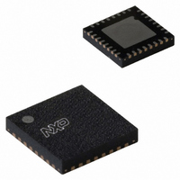
SC68C752BIBS,157 NXP Semiconductors, SC68C752BIBS,157 Datasheet - Page 22

SC68C752BIBS,157
Manufacturer Part Number
SC68C752BIBS,157
Description
IC UART DUAL 32HVQFN
Manufacturer
NXP Semiconductors
Datasheet
1.SC68C752BIBS128.pdf
(48 pages)
Specifications of SC68C752BIBS,157
Number Of Channels
2, DUART
Fifo's
64 Byte
Voltage - Supply
2.5V, 3.3V, 5V
With Auto Flow Control
Yes
With False Start Bit Detection
Yes
With Modem Control
Yes
Mounting Type
Surface Mount
Package / Case
32-VFQFN Exposed Pad
Lead Free Status / RoHS Status
Lead free / RoHS Compliant
Other names
935280969157
SC68C752BIBS
SC68C752BIBS
SC68C752BIBS
SC68C752BIBS
NXP Semiconductors
SC68C752B_4
Product data sheet
7.3 FIFO Control Register (FCR)
This is a write-only register that is used for enabling the FIFOs, clearing the FIFOs, setting
transmitter and receiver trigger levels, and selecting the type of DMA signalling.
shows FIFO Control Register bit settings.
Table 12.
Bit
7:6
5:4
3
2
1
0
Symbol
FCR[7] (MSB),
FCR[6] (LSB)
FCR[5] (MSB),
FCR[4] (LSB)
FCR[3]
FCR[2]
FCR[1]
FCR[0]
FIFO Control Register bits description
5 V, 3.3 V and 2.5 V dual UART, 5 Mbit/s (max.), with 64-byte FIFOs
Rev. 04 — 20 January 2010
Description
RX trigger. Sets the trigger level for the receive FIFO.
TX trigger. Sets the trigger level for the transmit FIFO.
FCR[5:4] can only be modified and enabled when EFR[4] is set. This is
because the transmit trigger level is regarded as an enhanced function.
DMA mode select.
Reset transmit FIFO.
Reset receive FIFO.
FIFO enable.
00 - 8 characters
01 - 16 characters
10 - 56 characters
11 - 60 characters
00 - 8 spaces
01 - 16 spaces
10 - 32 spaces
11 - 56 spaces
logic 0 = Set DMA mode ‘0’
logic 1 = Set DMA mode ‘1’
logic 0 = No FIFO transmit reset (normal default condition)
logic 1 = Clears the contents of the transmit FIFO and resets the FIFO
counter logic (the transmit shift register is not cleared or altered). This
bit will return to a logic 0 after clearing the FIFO.
logic 0 = no FIFO receive reset (normal default condition)
logic 1 = Clears the contents of the receive FIFO and resets the FIFO
counter logic (the receive shift register is not cleared or altered). This
bit will return to a logic 0 after clearing the FIFO.
logic 0 = disable the transmit and receive FIFO (normal default
condition)
logic 1 = enable the transmit and receive FIFO
SC68C752B
© NXP B.V. 2010. All rights reserved.
Table 12
22 of 48


