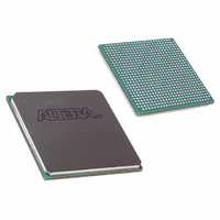
EP1SGX25CF672C7 Altera, EP1SGX25CF672C7 Datasheet - Page 203

EP1SGX25CF672C7
Manufacturer Part Number
EP1SGX25CF672C7
Description
IC STRATIX GX FPGA 25KLE 672FBGA
Manufacturer
Altera
Series
Stratix® GXr
Datasheet
1.EP1SGX10CF672C7N.pdf
(272 pages)
Specifications of EP1SGX25CF672C7
Number Of Logic Elements/cells
25660
Number Of Labs/clbs
2566
Total Ram Bits
1944576
Number Of I /o
455
Voltage - Supply
1.425 V ~ 1.575 V
Mounting Type
Surface Mount
Operating Temperature
0°C ~ 85°C
Package / Case
672-FBGA
Family Name
Stratix GX
Number Of Logic Blocks/elements
25660
# I/os (max)
455
Frequency (max)
4.38597GHz
Process Technology
SRAM
Operating Supply Voltage (typ)
1.5V
Logic Cells
25660
Ram Bits
1944576
Operating Supply Voltage (min)
1.425V
Operating Supply Voltage (max)
1.575V
Operating Temp Range
0C to 85C
Operating Temperature Classification
Commercial
Mounting
Surface Mount
Pin Count
672
Package Type
FC-FBGA
Lead Free Status / RoHS Status
Contains lead / RoHS non-compliant
Number Of Gates
-
Lead Free Status / Rohs Status
Not Compliant
Available stocks
Company
Part Number
Manufacturer
Quantity
Price
Part Number:
EP1SGX25CF672C7
Manufacturer:
ALTERA/阿尔特拉
Quantity:
20 000
- Current page: 203 of 272
- Download datasheet (3Mb)
Operating
Conditions
Altera Corporation
June 2006
V
V
V
I
T
T
T
V
V
V
SGX51006-1.2
OUT
Table 6–1. Stratix GX Device Absolute Maximum Ratings
Table 6–2. Stratix GX Device Recommended Operating Conditions (Part 1 of 2)
AMB
Symbol
STG
J
CCINT
CCIO
I
CCINT
CCIO
I
Symbol
Supply voltage
DC input voltage
DC output current, per pin
Storage temperature
Ambient temperature
Junction temperature
Supply voltage for internal logic
and input buffers
Supply voltage for output buffers,
3.3-V operation
Supply voltage for output buffers,
2.5-V operation
Supply voltage for output buffers,
1.8-V operation
Supply voltage for output buffers,
1.5-V operation
Input voltage
Parameter
Parameter
Stratix
However, industrial-grade devices may have limited speed-grade
availability.
Tables 6–1
ratings, recommended operating conditions, DC operating conditions,
and transceiver block absolute maximum ratings. Notes for
through
immediately follow that table, and notes for
immediately follow
®
GX devices are offered in both commercial and industrial grades.
6–6
through
With respect to ground
No bias
Under bias
BGA packages under bias
immediately follow
(4)
(4),
(4)
(4)
(4)
(3),
6–12
Conditions
Table
Conditions
(5)
(6)
provide information on absolute maximum
6–12.
Notes
(3)
Table
(1),
6. DC & Switching
3.00 (3.135)
6–6, notes for
Minimum
Minimum
(2)
1.425
2.375
1.71
–0.5
1.4
–0.5
–0.5
–0.5
–25
–65
–65
Characteristics
Tables 6–8
Note
3.60 (3.465)
Table 6–7
Maximum
Maximum
through
1.575
2.625
150
135
135
2.4
4.6
4.6
(7), (12),
1.89
25
1.6
4.1
Tables 6–1
6–12
(13)
Unit
mA
° C
° C
° C
Unit
V
V
V
V
V
V
V
V
V
6–1
Related parts for EP1SGX25CF672C7
Image
Part Number
Description
Manufacturer
Datasheet
Request
R

Part Number:
Description:
CYCLONE II STARTER KIT EP2C20N
Manufacturer:
Altera
Datasheet:

Part Number:
Description:
CPLD, EP610 Family, ECMOS Process, 300 Gates, 16 Macro Cells, 16 Reg., 16 User I/Os, 5V Supply, 35 Speed Grade, 24DIP
Manufacturer:
Altera Corporation
Datasheet:

Part Number:
Description:
CPLD, EP610 Family, ECMOS Process, 300 Gates, 16 Macro Cells, 16 Reg., 16 User I/Os, 5V Supply, 15 Speed Grade, 24DIP
Manufacturer:
Altera Corporation
Datasheet:

Part Number:
Description:
Manufacturer:
Altera Corporation
Datasheet:

Part Number:
Description:
CPLD, EP610 Family, ECMOS Process, 300 Gates, 16 Macro Cells, 16 Reg., 16 User I/Os, 5V Supply, 30 Speed Grade, 24DIP
Manufacturer:
Altera Corporation
Datasheet:

Part Number:
Description:
High-performance, low-power erasable programmable logic devices with 8 macrocells, 10ns
Manufacturer:
Altera Corporation
Datasheet:

Part Number:
Description:
High-performance, low-power erasable programmable logic devices with 8 macrocells, 7ns
Manufacturer:
Altera Corporation
Datasheet:

Part Number:
Description:
Classic EPLD
Manufacturer:
Altera Corporation
Datasheet:

Part Number:
Description:
High-performance, low-power erasable programmable logic devices with 8 macrocells, 10ns
Manufacturer:
Altera Corporation
Datasheet:

Part Number:
Description:
Manufacturer:
Altera Corporation
Datasheet:

Part Number:
Description:
Manufacturer:
Altera Corporation
Datasheet:

Part Number:
Description:
Manufacturer:
Altera Corporation
Datasheet:

Part Number:
Description:
CPLD, EP610 Family, ECMOS Process, 300 Gates, 16 Macro Cells, 16 Reg., 16 User I/Os, 5V Supply, 25 Speed Grade, 24DIP
Manufacturer:
Altera Corporation
Datasheet:


