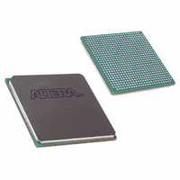
EP1SGX25CF672C7 Altera, EP1SGX25CF672C7 Datasheet - Page 18

EP1SGX25CF672C7
Manufacturer Part Number
EP1SGX25CF672C7
Description
IC STRATIX GX FPGA 25KLE 672FBGA
Manufacturer
Altera
Series
Stratix® GXr
Datasheet
1.EP1SGX10CF672C7N.pdf
(272 pages)
Specifications of EP1SGX25CF672C7
Number Of Logic Elements/cells
25660
Number Of Labs/clbs
2566
Total Ram Bits
1944576
Number Of I /o
455
Voltage - Supply
1.425 V ~ 1.575 V
Mounting Type
Surface Mount
Operating Temperature
0°C ~ 85°C
Package / Case
672-FBGA
Family Name
Stratix GX
Number Of Logic Blocks/elements
25660
# I/os (max)
455
Frequency (max)
4.38597GHz
Process Technology
SRAM
Operating Supply Voltage (typ)
1.5V
Logic Cells
25660
Ram Bits
1944576
Operating Supply Voltage (min)
1.425V
Operating Supply Voltage (max)
1.575V
Operating Temp Range
0C to 85C
Operating Temperature Classification
Commercial
Mounting
Surface Mount
Pin Count
672
Package Type
FC-FBGA
Lead Free Status / RoHS Status
Contains lead / RoHS non-compliant
Number Of Gates
-
Lead Free Status / Rohs Status
Not Compliant
Available stocks
Company
Part Number
Manufacturer
Quantity
Price
Part Number:
EP1SGX25CF672C7
Manufacturer:
ALTERA/阿尔特拉
Quantity:
20 000
- Current page: 18 of 272
- Download datasheet (3Mb)
2–8
Stratix GX Device Handbook, Volume 1
8B/10B Encoder
The 8B/10B encoder translates 8-bit wide data + 1 control enable bit into
a 10-bit encoded data. The encoded data has a maximum run length of 5.
The 8B/10B encoder can be bypassed.
process.
Figure 2–4. Encoding Process
Transmit State Machine
The transmit state machine operates in either XAUI mode or in GIGE
mode, depending on the protocol used.
GIGE Mode
In GIGE mode, the transmit state machines convert all idle ordered sets
(/K28.5/, /Dx.y/) to either /I1/ or /I2/ ordered sets. /I1/ consists
of a negative-ending disparity /K28.5/ (denoted by /K28.5/-)
followed by a neutral /D5.6/. /I2/ consists of a positive-ending
disparity /K28.5/ (denoted by /K28.5/+) and a negative-ending
disparity /D16.2/ (denoted by /D16.2/-). The transmit state machines
do not convert any of the ordered sets to match /C1/ or /C2/, which are
the configuration ordered sets. (/C1/ and /C2/ are defined by
(/K28.5/, /D21.5/) and (/K28.5/, /D2.2/), respectively.) Both the
/I1/ and /I2/ ordered sets guarantee a negative-ending disparity after
each ordered set. The GIGE transmit state machine can be statically
disabled in the Quartus II software, even if using the GIGE protocol
mode.
MSB sent last
9
j
h
8
H
7
g
7
G
6
8b-10b conversion
6
5
F
f
E
5
4
i
3
D
Figure 2–4
e
4
2
C
d
3
B
1
c
2
diagrams the encoding
0
A
LSB sent first
b
1
Altera Corporation
+
a
0
ctrl
June 2006
Related parts for EP1SGX25CF672C7
Image
Part Number
Description
Manufacturer
Datasheet
Request
R

Part Number:
Description:
CYCLONE II STARTER KIT EP2C20N
Manufacturer:
Altera
Datasheet:

Part Number:
Description:
CPLD, EP610 Family, ECMOS Process, 300 Gates, 16 Macro Cells, 16 Reg., 16 User I/Os, 5V Supply, 35 Speed Grade, 24DIP
Manufacturer:
Altera Corporation
Datasheet:

Part Number:
Description:
CPLD, EP610 Family, ECMOS Process, 300 Gates, 16 Macro Cells, 16 Reg., 16 User I/Os, 5V Supply, 15 Speed Grade, 24DIP
Manufacturer:
Altera Corporation
Datasheet:

Part Number:
Description:
Manufacturer:
Altera Corporation
Datasheet:

Part Number:
Description:
CPLD, EP610 Family, ECMOS Process, 300 Gates, 16 Macro Cells, 16 Reg., 16 User I/Os, 5V Supply, 30 Speed Grade, 24DIP
Manufacturer:
Altera Corporation
Datasheet:

Part Number:
Description:
High-performance, low-power erasable programmable logic devices with 8 macrocells, 10ns
Manufacturer:
Altera Corporation
Datasheet:

Part Number:
Description:
High-performance, low-power erasable programmable logic devices with 8 macrocells, 7ns
Manufacturer:
Altera Corporation
Datasheet:

Part Number:
Description:
Classic EPLD
Manufacturer:
Altera Corporation
Datasheet:

Part Number:
Description:
High-performance, low-power erasable programmable logic devices with 8 macrocells, 10ns
Manufacturer:
Altera Corporation
Datasheet:

Part Number:
Description:
Manufacturer:
Altera Corporation
Datasheet:

Part Number:
Description:
Manufacturer:
Altera Corporation
Datasheet:

Part Number:
Description:
Manufacturer:
Altera Corporation
Datasheet:

Part Number:
Description:
CPLD, EP610 Family, ECMOS Process, 300 Gates, 16 Macro Cells, 16 Reg., 16 User I/Os, 5V Supply, 25 Speed Grade, 24DIP
Manufacturer:
Altera Corporation
Datasheet:


