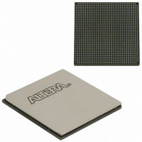
EP1AGX90EF1152I6N Altera, EP1AGX90EF1152I6N Datasheet - Page 99

EP1AGX90EF1152I6N
Manufacturer Part Number
EP1AGX90EF1152I6N
Description
IC ARRIA GX FPGA 90K 1152FBGA
Manufacturer
Altera
Series
Arria GXr
Datasheet
1.EP1AGX20CF484C6N.pdf
(234 pages)
Specifications of EP1AGX90EF1152I6N
Number Of Logic Elements/cells
90220
Number Of Labs/clbs
4511
Total Ram Bits
4477824
Number Of I /o
538
Voltage - Supply
1.15 V ~ 1.25 V
Mounting Type
Surface Mount
Operating Temperature
-40°C ~ 100°C
Package / Case
1152-FBGA
Lead Free Status / RoHS Status
Lead free / RoHS Compliant
Number Of Gates
-
Other names
544-2387
Available stocks
Company
Part Number
Manufacturer
Quantity
Price
- Current page: 99 of 234
- Download datasheet (4Mb)
Chapter 2: Arria GX Architecture
I/O Structure
Programmable Pull-Up Resistor
Advanced I/O Standard Support
© December 2009 Altera Corporation
f
For the specific sustaining current driven through this resistor and overdrive current
used to identify the next-driven input level, refer to the
chapter.
Each Arria GX device I/O pin provides an optional programmable pull-up resistor
during user mode. If you enable this feature for an I/O pin, the pull-up resistor
(typically 25 k) holds the output to the V
Arria GX device IOEs support the following I/O standards:
■
■
■
■
■
■
■
■
■
■
■
■
■
■
■
■
■
3.3-V LVTTL/LVCMOS
2.5-V LVTTL/LVCMOS
1.8-V LVTTL/LVCMOS
1.5-V LVCMOS
3.3-V PCI
3.3-V PCI-X mode 1
LVDS
LVPECL (on input and output clocks only)
Differential 1.5-V HSTL class I and II
Differential 1.8-V HSTL class I and II
Differential SSTL-18 class I and II
Differential SSTL-2 class I and II
1.2-V HSTL class I and II
1.5-V HSTL class I and II
1.8-V HSTL class I and II
SSTL-2 class I and II
SSTL-18 class I and II
CCIO
level of the output pin’s bank.
DC & Switching Characteristics
Arria GX Device Handbook, Volume 1
2–93
Related parts for EP1AGX90EF1152I6N
Image
Part Number
Description
Manufacturer
Datasheet
Request
R

Part Number:
Description:
CYCLONE II STARTER KIT EP2C20N
Manufacturer:
Altera
Datasheet:

Part Number:
Description:
CPLD, EP610 Family, ECMOS Process, 300 Gates, 16 Macro Cells, 16 Reg., 16 User I/Os, 5V Supply, 35 Speed Grade, 24DIP
Manufacturer:
Altera Corporation
Datasheet:

Part Number:
Description:
CPLD, EP610 Family, ECMOS Process, 300 Gates, 16 Macro Cells, 16 Reg., 16 User I/Os, 5V Supply, 15 Speed Grade, 24DIP
Manufacturer:
Altera Corporation
Datasheet:

Part Number:
Description:
Manufacturer:
Altera Corporation
Datasheet:

Part Number:
Description:
CPLD, EP610 Family, ECMOS Process, 300 Gates, 16 Macro Cells, 16 Reg., 16 User I/Os, 5V Supply, 30 Speed Grade, 24DIP
Manufacturer:
Altera Corporation
Datasheet:

Part Number:
Description:
High-performance, low-power erasable programmable logic devices with 8 macrocells, 10ns
Manufacturer:
Altera Corporation
Datasheet:

Part Number:
Description:
High-performance, low-power erasable programmable logic devices with 8 macrocells, 7ns
Manufacturer:
Altera Corporation
Datasheet:

Part Number:
Description:
Classic EPLD
Manufacturer:
Altera Corporation
Datasheet:

Part Number:
Description:
High-performance, low-power erasable programmable logic devices with 8 macrocells, 10ns
Manufacturer:
Altera Corporation
Datasheet:

Part Number:
Description:
Manufacturer:
Altera Corporation
Datasheet:

Part Number:
Description:
Manufacturer:
Altera Corporation
Datasheet:

Part Number:
Description:
Manufacturer:
Altera Corporation
Datasheet:

Part Number:
Description:
CPLD, EP610 Family, ECMOS Process, 300 Gates, 16 Macro Cells, 16 Reg., 16 User I/Os, 5V Supply, 25 Speed Grade, 24DIP
Manufacturer:
Altera Corporation
Datasheet:


