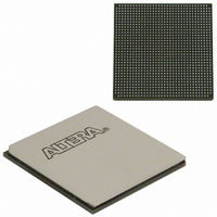
EP1AGX90EF1152I6N Altera, EP1AGX90EF1152I6N Datasheet - Page 97

EP1AGX90EF1152I6N
Manufacturer Part Number
EP1AGX90EF1152I6N
Description
IC ARRIA GX FPGA 90K 1152FBGA
Manufacturer
Altera
Series
Arria GXr
Datasheet
1.EP1AGX20CF484C6N.pdf
(234 pages)
Specifications of EP1AGX90EF1152I6N
Number Of Logic Elements/cells
90220
Number Of Labs/clbs
4511
Total Ram Bits
4477824
Number Of I /o
538
Voltage - Supply
1.15 V ~ 1.25 V
Mounting Type
Surface Mount
Operating Temperature
-40°C ~ 100°C
Package / Case
1152-FBGA
Lead Free Status / RoHS Status
Lead free / RoHS Compliant
Number Of Gates
-
Other names
544-2387
Available stocks
Company
Part Number
Manufacturer
Quantity
Price
- Current page: 97 of 234
- Download datasheet (4Mb)
Chapter 2: Arria GX Architecture
I/O Structure
Figure 2–77. DQS Phase-Shift Circuitry
Notes to
(1) There are up to 18 pairs of DQS pins available on the top or bottom of the Arria GX device. There are up to 10 pairs on the right side and 8 pairs
(2) The “t” module represents the DQS logic block.
(3) Clock pins CLK[15..12]p feed phase-shift circuitry on the top of the device and clock pins CLK[7..4]p feed the phase circuitry on the
(4) You can only use PLL 5 to feed the DQS phase-shift circuitry on the top of the device and PLL 6 to feed the DQS phase-shift circuitry on the bottom
Programmable Drive Strength
© December 2009 Altera Corporation
on the left side of the DQS phase-shift circuitry.
bottom of the device. You can also use a PLL clock output as a reference clock to phase shift circuitry.
of the device.
Figure
f
2–77:
to IOE
DQS
Pin
Dt
The Arria GX device has two phase-shifting reference circuits, one on the top and one
on the bottom of the device. The circuit on the top controls the compensated delay
elements for all DQS pins on the top. The circuit on the bottom controls the
compensated delay elements for all DQS pins on the bottom.
Each phase-shifting reference circuit is driven by a system reference clock, which must
have the same frequency as the DQS signal. Clock pins CLK[15..12]p feed phase
circuitry on the top of the device and clock pins CLK[7..4]p feed phase circuitry on
the bottom of the device. In addition, PLL clock outputs can also feed the
phase-shifting reference circuits.
control of each DQS delay shift on the top of the device. This same circuit is
duplicated on the bottom of the device.
These dedicated circuits combined with enhanced PLL clocking and phase-shift
ability provide a complete hardware solution for interfacing to high-speed memory.
For more information about external memory interfaces, refer to the
Interfaces in Arria GX Devices
The output buffer for each Arria GX device I/O pin has a programmable drive
strength control for certain I/O standards. The LVTTL, LVCMOS, SSTL, and HSTL
standards have several levels of drive strength that you can control. The default
setting used in the Quartus II software is the maximum current strength setting that is
used to achieve maximum I/O performance. For all I/O standards, the minimum
setting is the lowest drive strength that guarantees the I
minimum settings provides signal slew rate control to reduce system noise and signal
overshoot.
(Note
to IOE
DQS
Pin
Dt
1),
(2)
CLK[15..12]p (3)
Phase-Shift
chapter.
Circuitry
DQS
Figure 2–77
From PLL 5 (4)
to IOE
DQS
Pin
Dt
shows the phase-shift reference circuit
OH
/I
Arria GX Device Handbook, Volume 1
OL
of the standard. Using
to IOE
DQS
Pin
External Memory
Dt
2–91
Related parts for EP1AGX90EF1152I6N
Image
Part Number
Description
Manufacturer
Datasheet
Request
R

Part Number:
Description:
CYCLONE II STARTER KIT EP2C20N
Manufacturer:
Altera
Datasheet:

Part Number:
Description:
CPLD, EP610 Family, ECMOS Process, 300 Gates, 16 Macro Cells, 16 Reg., 16 User I/Os, 5V Supply, 35 Speed Grade, 24DIP
Manufacturer:
Altera Corporation
Datasheet:

Part Number:
Description:
CPLD, EP610 Family, ECMOS Process, 300 Gates, 16 Macro Cells, 16 Reg., 16 User I/Os, 5V Supply, 15 Speed Grade, 24DIP
Manufacturer:
Altera Corporation
Datasheet:

Part Number:
Description:
Manufacturer:
Altera Corporation
Datasheet:

Part Number:
Description:
CPLD, EP610 Family, ECMOS Process, 300 Gates, 16 Macro Cells, 16 Reg., 16 User I/Os, 5V Supply, 30 Speed Grade, 24DIP
Manufacturer:
Altera Corporation
Datasheet:

Part Number:
Description:
High-performance, low-power erasable programmable logic devices with 8 macrocells, 10ns
Manufacturer:
Altera Corporation
Datasheet:

Part Number:
Description:
High-performance, low-power erasable programmable logic devices with 8 macrocells, 7ns
Manufacturer:
Altera Corporation
Datasheet:

Part Number:
Description:
Classic EPLD
Manufacturer:
Altera Corporation
Datasheet:

Part Number:
Description:
High-performance, low-power erasable programmable logic devices with 8 macrocells, 10ns
Manufacturer:
Altera Corporation
Datasheet:

Part Number:
Description:
Manufacturer:
Altera Corporation
Datasheet:

Part Number:
Description:
Manufacturer:
Altera Corporation
Datasheet:

Part Number:
Description:
Manufacturer:
Altera Corporation
Datasheet:

Part Number:
Description:
CPLD, EP610 Family, ECMOS Process, 300 Gates, 16 Macro Cells, 16 Reg., 16 User I/Os, 5V Supply, 25 Speed Grade, 24DIP
Manufacturer:
Altera Corporation
Datasheet:


