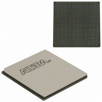
EP1AGX90EF1152I6N Altera, EP1AGX90EF1152I6N Datasheet - Page 150

EP1AGX90EF1152I6N
Manufacturer Part Number
EP1AGX90EF1152I6N
Description
IC ARRIA GX FPGA 90K 1152FBGA
Manufacturer
Altera
Series
Arria GXr
Datasheet
1.EP1AGX20CF484C6N.pdf
(234 pages)
Specifications of EP1AGX90EF1152I6N
Number Of Logic Elements/cells
90220
Number Of Labs/clbs
4511
Total Ram Bits
4477824
Number Of I /o
538
Voltage - Supply
1.15 V ~ 1.25 V
Mounting Type
Surface Mount
Operating Temperature
-40°C ~ 100°C
Package / Case
1152-FBGA
Lead Free Status / RoHS Status
Lead free / RoHS Compliant
Number Of Gates
-
Other names
544-2387
Available stocks
Company
Part Number
Manufacturer
Quantity
Price
- Current page: 150 of 234
- Download datasheet (4Mb)
4–28
Table 4–44. Output Timing Measurement Methodology for Output Pins
Arria GX Device Handbook, Volume 1
LVTTL
LVCMOS
2.5 V
1.8 V
1.5 V
PCI
PCI-X
SSTL-2 Class I
SSTL-2 Class II
SSTL-18 Class I
SSTL-18 Class II
1.8-V HSTL Class I
1.8-V HSTL Class II
1.5-V HSTL Class I
1.5-V HSTL Class II
1.2-V HSTL with OCT
Differential SSTL-2 Class I
Differential SSTL-2 Class II
Differential SSTL-18 Class I
Differential SSTL-18 Class II
1.5-V differential HSTL Class I
1.5-V differential HSTL Class II
1.8-V differential HSTL Class I
(5)
(4)
(4)
(4)
(5)
(4)
(4)
I/O Standard
Figure 4–7. Output Delay Timing Reporting Setup Modeled by Quartus II
Notes to
(1) Output pin timing is reported at the output pin of the FPGA device. Additional delays for loading and board trace delay
(2) V
(3) V
need to be accounted for with IBIS model simulations.
CCPD
CCINT
Figure
is 3.085 V unless otherwise specified.
is 1.12 V unless otherwise specified.
4–7:
R
Output
Buffer
V
S
—
—
—
—
—
—
—
25
25
25
25
—
—
—
—
—
25
25
50
25
—
—
—
GND
CCIO
(
)
Output
R
D
—
—
—
—
—
—
—
—
—
—
—
—
—
—
—
—
—
—
—
—
—
—
—
V
(
MEAS
)
Loading and Termination
R
T
—
—
—
—
—
—
—
50
25
50
25
50
25
50
25
—
50
25
50
25
50
25
50
R
(
S
)
V
GND
TT
(Note
R
C
3.135
3.135
2.375
1.710
1.425
2.970
2.970
2.325
2.325
1.660
1.660
1.660
1.660
1.375
1.375
1.140
2.325
2.325
1.660
1.660
1.375
1.375
1.660
V
T
L
(V)
CCIO
1), (2),
V
Chapter 4: DC and Switching Characteristics
1.123
1.123
0.790
0.790
0.790
0.790
0.648
0.648
1.123
1.123
0.790
0.790
0.648
0.648
0.790
TT
—
—
—
—
—
—
—
—
(3)
(V)
© December 2009 Altera Corporation
Output
Output
C
L
10
10
(pF)
0
0
0
0
0
0
0
0
0
0
0
0
0
0
0
0
0
0
0
0
0
p
n
R
D
Measurement
V
I/O Timing Model
0.6875
MEAS
1.5675
1.5675
1.1875
0.7125
1.1625
1.1625
0.6875
0.6875
1.1625
1.1625
0.6875
0.855
1.485
1.485
0.570
Point
0.83
0.83
0.83
0.83
0.83
0.83
0.83
(V)
Related parts for EP1AGX90EF1152I6N
Image
Part Number
Description
Manufacturer
Datasheet
Request
R

Part Number:
Description:
CYCLONE II STARTER KIT EP2C20N
Manufacturer:
Altera
Datasheet:

Part Number:
Description:
CPLD, EP610 Family, ECMOS Process, 300 Gates, 16 Macro Cells, 16 Reg., 16 User I/Os, 5V Supply, 35 Speed Grade, 24DIP
Manufacturer:
Altera Corporation
Datasheet:

Part Number:
Description:
CPLD, EP610 Family, ECMOS Process, 300 Gates, 16 Macro Cells, 16 Reg., 16 User I/Os, 5V Supply, 15 Speed Grade, 24DIP
Manufacturer:
Altera Corporation
Datasheet:

Part Number:
Description:
Manufacturer:
Altera Corporation
Datasheet:

Part Number:
Description:
CPLD, EP610 Family, ECMOS Process, 300 Gates, 16 Macro Cells, 16 Reg., 16 User I/Os, 5V Supply, 30 Speed Grade, 24DIP
Manufacturer:
Altera Corporation
Datasheet:

Part Number:
Description:
High-performance, low-power erasable programmable logic devices with 8 macrocells, 10ns
Manufacturer:
Altera Corporation
Datasheet:

Part Number:
Description:
High-performance, low-power erasable programmable logic devices with 8 macrocells, 7ns
Manufacturer:
Altera Corporation
Datasheet:

Part Number:
Description:
Classic EPLD
Manufacturer:
Altera Corporation
Datasheet:

Part Number:
Description:
High-performance, low-power erasable programmable logic devices with 8 macrocells, 10ns
Manufacturer:
Altera Corporation
Datasheet:

Part Number:
Description:
Manufacturer:
Altera Corporation
Datasheet:

Part Number:
Description:
Manufacturer:
Altera Corporation
Datasheet:

Part Number:
Description:
Manufacturer:
Altera Corporation
Datasheet:

Part Number:
Description:
CPLD, EP610 Family, ECMOS Process, 300 Gates, 16 Macro Cells, 16 Reg., 16 User I/Os, 5V Supply, 25 Speed Grade, 24DIP
Manufacturer:
Altera Corporation
Datasheet:


