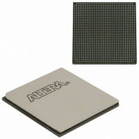
EP1AGX90EF1152I6N Altera, EP1AGX90EF1152I6N Datasheet - Page 228

EP1AGX90EF1152I6N
Manufacturer Part Number
EP1AGX90EF1152I6N
Description
IC ARRIA GX FPGA 90K 1152FBGA
Manufacturer
Altera
Series
Arria GXr
Datasheet
1.EP1AGX20CF484C6N.pdf
(234 pages)
Specifications of EP1AGX90EF1152I6N
Number Of Logic Elements/cells
90220
Number Of Labs/clbs
4511
Total Ram Bits
4477824
Number Of I /o
538
Voltage - Supply
1.15 V ~ 1.25 V
Mounting Type
Surface Mount
Operating Temperature
-40°C ~ 100°C
Package / Case
1152-FBGA
Lead Free Status / RoHS Status
Lead free / RoHS Compliant
Number Of Gates
-
Other names
544-2387
Available stocks
Company
Part Number
Manufacturer
Quantity
Price
- Current page: 228 of 234
- Download datasheet (4Mb)
4–106
JTAG Timing Specifications
Figure 4–13. Arria GX JTAG Waveforms.
Arria GX Device Handbook, Volume 1
Captured
Table 4–121. DQS Bus Clock Skew Adder Specifications (t
Table 4–122. DQS Phase Offset Delay Per Stage (ps)
Figure 4–13
Notes to
(1) The delay settings are linear.
(2) The valid settings for phase offset are –32 to +31.
(3) The typical value equals the average of the minimum and maximum values.
Driven
Signal
Signal
to be
to be
TMS
TDO
TCK
TDI
Speed Grade
–6
Table
18 DQ per DQS
36 DQ per DQS
4 DQ per DQS
9 DQ per DQS
shows the timing requirements for the JTAG signals
t
Mode
4–122:
JCH
t
t
JPZX
JSZX
t
JCP
t
JSSU
t
JCL
Min
10
t
JSH
Positive Offset
t
t
JPCO
JSCO
t
JPSU
DQS Clock Skew Adder (ps)
Max
16
t
t
JSXZ
JPH
Note (1), (2), (3)
DQS_CLOCK_SKEW_A DDER
40
70
75
95
Chapter 4: DC and Switching Characteristics
t
JPXZ
© December 2009 Altera Corporation
Min
8
Negative Offset
JTAG Timing Specifications
)
Max
12
Related parts for EP1AGX90EF1152I6N
Image
Part Number
Description
Manufacturer
Datasheet
Request
R

Part Number:
Description:
CYCLONE II STARTER KIT EP2C20N
Manufacturer:
Altera
Datasheet:

Part Number:
Description:
CPLD, EP610 Family, ECMOS Process, 300 Gates, 16 Macro Cells, 16 Reg., 16 User I/Os, 5V Supply, 35 Speed Grade, 24DIP
Manufacturer:
Altera Corporation
Datasheet:

Part Number:
Description:
CPLD, EP610 Family, ECMOS Process, 300 Gates, 16 Macro Cells, 16 Reg., 16 User I/Os, 5V Supply, 15 Speed Grade, 24DIP
Manufacturer:
Altera Corporation
Datasheet:

Part Number:
Description:
Manufacturer:
Altera Corporation
Datasheet:

Part Number:
Description:
CPLD, EP610 Family, ECMOS Process, 300 Gates, 16 Macro Cells, 16 Reg., 16 User I/Os, 5V Supply, 30 Speed Grade, 24DIP
Manufacturer:
Altera Corporation
Datasheet:

Part Number:
Description:
High-performance, low-power erasable programmable logic devices with 8 macrocells, 10ns
Manufacturer:
Altera Corporation
Datasheet:

Part Number:
Description:
High-performance, low-power erasable programmable logic devices with 8 macrocells, 7ns
Manufacturer:
Altera Corporation
Datasheet:

Part Number:
Description:
Classic EPLD
Manufacturer:
Altera Corporation
Datasheet:

Part Number:
Description:
High-performance, low-power erasable programmable logic devices with 8 macrocells, 10ns
Manufacturer:
Altera Corporation
Datasheet:

Part Number:
Description:
Manufacturer:
Altera Corporation
Datasheet:

Part Number:
Description:
Manufacturer:
Altera Corporation
Datasheet:

Part Number:
Description:
Manufacturer:
Altera Corporation
Datasheet:

Part Number:
Description:
CPLD, EP610 Family, ECMOS Process, 300 Gates, 16 Macro Cells, 16 Reg., 16 User I/Os, 5V Supply, 25 Speed Grade, 24DIP
Manufacturer:
Altera Corporation
Datasheet:


