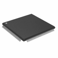
ADSP-21262SKSTZ200 Analog Devices Inc, ADSP-21262SKSTZ200 Datasheet - Page 7

ADSP-21262SKSTZ200
Manufacturer Part Number
ADSP-21262SKSTZ200
Description
IC DSP CONTROLLER 32BIT 144-LQFP
Manufacturer
Analog Devices Inc
Series
SHARC®r
Type
Fixed/Floating Pointr
Specifications of ADSP-21262SKSTZ200
Interface
DAI, SPI
Clock Rate
200MHz
Non-volatile Memory
ROM (512 kB)
On-chip Ram
256kB
Voltage - I/o
3.30V
Voltage - Core
1.20V
Operating Temperature
0°C ~ 70°C
Mounting Type
Surface Mount
Package / Case
144-LQFP
No. Of Bits
32 / 40
Frequency
200MHz
Supply Voltage
1.2V
Embedded Interface Type
Host Port, Serial
Supply Voltage Range
1.14V To 1.26V
Operating Temperature Range
0°C To +70°C
Package
144LQFP
Numeric And Arithmetic Format
Floating-Point
Maximum Speed
200 MHz
Ram Size
256 KB
Device Million Instructions Per Second
200 MIPS
Lead Free Status / RoHS Status
Lead free / RoHS Compliant
Other names
ADSP21262SKSTZ200
ADSP21262SKSTZ200
ADSP21262SKSTZ200
Available stocks
Company
Part Number
Manufacturer
Quantity
Price
Company:
Part Number:
ADSP-21262SKSTZ200
Manufacturer:
Analog Devices Inc
Quantity:
10 000
Left-justified sample pair mode is a mode where in each frame
sync cycle two samples of data are transmitted/received—one
sample on the high segment of the frame sync, the other on the
low segment of the frame sync. Programs have control over var-
ious attributes of this mode.
Each of the serial ports supports the left-justified sample pair
and I
monly used by audio codecs, ADCs, and DACs), with two data
pins, allowing four left-justified sample pair or I
(using two stereo devices) per serial port, with a maximum of up
NORMAL WORD
• I
• Left-justified sample pair mode
SHORT WORD
LONG WORD
ADDRESS
ADDRESS
ADDRESS
2
2
S protocols (I
S mode
SPACE
SPACE
SPACE
2
S is an industry-standard interface com-
INTERNAL MEMORY
BLOCK 0 SRAM (1M BIT)
BLOCK 1 SRAM (1M BIT)
BLOCK 0 ROM (2M BIT)
BLOCK 0 SRAM (1M BIT)
BLOCK 0 ROM (2M BIT) 2
BLOCK 1 SRAM (1M BIT)
BLOCK 1 ROM (2M BIT) 3
BLOCK 0 SRAM (1M BIT)
BLOCK 1 SRAM (1M BIT)
BLOCK 1 ROM (2M BIT)
BLOCK 0 ROM (2M BIT)
BLOCK 1 ROM (2M BIT)
IOP REGISTERS
RESERVED
RESERVED
RESERVED
RESERVED
RESERVED
RESERVED
SPACE
2
S channels
Figure 3. ADSP-21262 Memory Map
Rev. B | Page 7 of 48 | August 2005
0x0000 0000–0x0003 FFFF
0x0004 0000
0x0004 3FFF
0x0004 4000–0x0005 7FFF
0x0005 8000
0x0005 FFFF
0x0006 0000
0x0006 3FFF
0x0006 4000–0x0007 7FFF
0x0007 8000
0x0007 FFFF
0x0008 0000
0x0008 7FFF
0x0008 8000–0x000A FFFF
0x000B 0000
0x000B FFFF
0x000C 0000
0x000C 7FFF
0x000C 8000–0x000E FFFF
0x000F 0000
0x000F FFFF
0x0010 0000
0x0010 FFFF
0x0011 0000–0x0015 FFFF
0x0016 0000
0x0017 FFFF
0x0018 0000
0x0018 FFFF
0x0019 0000–0x001D FFFF
0x001E 0000
0x001F FFFF
ADDRESS
to 24 audio channels. The serial ports permit little-endian or
big-endian transmission formats and word lengths selectable
from 3 bits to 32 bits. For the left-justified sample pair and I
modes, data-word lengths are selectable between 8 bits and 32
bits. Serial ports offer selectable synchronization and transmit
modes as well as optional µ-law or A-law companding selection
on a per channel basis. Serial port clocks and frame syncs can be
internally or externally generated.
Serial Peripheral (Compatible) Interface
Serial peripheral interface is an industry-standard synchronous
serial link, enabling the ADSP-21262 SPI-compatible port to
communicate with other SPI-compatible devices. SPI is an
1 EXTERNAL MEMORY IS NOT DIRECTLY ACCESSIBLE BY THE
2 BLOCK 0 ROM HAS A 48-BIT ADDRESS RANGE
3 BLOCK 1 ROM HAS A 48-BIT ADDRESS RANGE
4 USE THE EXTERNAL ADDRESSES LISTED HERE WITH THE
CORE. DMA MUST BE USED TO READ OR WRITE TO THIS
MEMORY USING THE SPI OR PARALLEL PORT.
(0x000A 0000–0x000A AAAA).
(0x000E 0000–0x000E AAAA).
PARALLEL PORT DMA REGISTERS. THE PARALLEL PORT
GENERATES ADDRESS WITHIN THE RANGE
0x0000 0000–0x00FF FFFF.
EXTERNAL MEMORY
ADDRESS SPACE 1, 4
EXTERNAL DMA
RESERVED
RESERVED
SPACE
ADSP-21262
ADDRESS
0x0020 0000
0x00FF FFFF
0x0100 0000
0x02FF FFFF
0x0300 0000
0x3FFF FFFF
2
S


