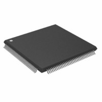
ADSP-21262SKSTZ200 Analog Devices Inc, ADSP-21262SKSTZ200 Datasheet - Page 2

ADSP-21262SKSTZ200
Manufacturer Part Number
ADSP-21262SKSTZ200
Description
IC DSP CONTROLLER 32BIT 144-LQFP
Manufacturer
Analog Devices Inc
Series
SHARC®r
Type
Fixed/Floating Pointr
Specifications of ADSP-21262SKSTZ200
Interface
DAI, SPI
Clock Rate
200MHz
Non-volatile Memory
ROM (512 kB)
On-chip Ram
256kB
Voltage - I/o
3.30V
Voltage - Core
1.20V
Operating Temperature
0°C ~ 70°C
Mounting Type
Surface Mount
Package / Case
144-LQFP
No. Of Bits
32 / 40
Frequency
200MHz
Supply Voltage
1.2V
Embedded Interface Type
Host Port, Serial
Supply Voltage Range
1.14V To 1.26V
Operating Temperature Range
0°C To +70°C
Package
144LQFP
Numeric And Arithmetic Format
Floating-Point
Maximum Speed
200 MHz
Ram Size
256 KB
Device Million Instructions Per Second
200 MIPS
Lead Free Status / RoHS Status
Lead free / RoHS Compliant
Other names
ADSP21262SKSTZ200
ADSP21262SKSTZ200
ADSP21262SKSTZ200
Available stocks
Company
Part Number
Manufacturer
Quantity
Price
Company:
Part Number:
ADSP-21262SKSTZ200
Manufacturer:
Analog Devices Inc
Quantity:
10 000
ADSP-21262
ADDITIONAL KEY FEATURES
2M bit on-chip dual-ported SRAM (1M bit block 0, 1M bit
4M bit on-chip dual-ported mask-programmable ROM
Dual data address generators (DAGs) with modulo and bit-
Zero-overhead looping with single-cycle loop setup,
Single-instruction multiple-data (SIMD) architecture
Accelerated FFT butterfly computation through a multiply
DMA controller supports:
JTAG background telemetry for enhanced emulation
IEEE 1149.1 JTAG standard test access port and on-chip
Dual voltage: 3.3 V I/O, 1.2 V core
Available in 136-ball BGA and 144-lead LQFP packages
Digital applications interface includes six serial ports, two
Asynchronous parallel/external port provides:
block 1) for simultaneous access by core processor and
DMA
(2M bit in block 0 and 2M bit in block 1)
reverse addressing
providing efficient program sequencing
provides:
Two computational processing elements
Concurrent execution—each processing element executes
Parallelism in buses and computational units allows single
with add and subtract instruction
22 zero-overhead DMA channels for transfers between the
32-bit background DMA transfers at core clock speed, in
features
emulation
Also available in lead-free packages
precision clock generators, an input data port, three pro-
grammable timers, and a signal routing unit
Access to asynchronous external memory
16 multiplexed address/data lines that can support 24-bit
66M byte/sec transfer rate for 200 MHz core rate
50M byte/sec transfer rate for 150 MHz core rate
256 word page boundaries
External memory access in a dedicated DMA channel
8-bit to 32-bit and 16-bit to 32-bit word packing options
Programmable wait state options: 2 to 31 CCLK
the same instruction, but operates on different data
cycle executions (with or without SIMD) of a multiply
operation; an ALU operation; a dual memory read or
write; and an instruction fetch
ADSP-21262 internal memory and serial ports (12), the
input data port (IDP) (eight), the SPI-compatible port
(one), and the parallel port (one)
parallel with full-speed processor execution
address external address range with 8-bit data or 16-bit
address external address range with 16-bit data
Rev. B | Page 2 of 48 | August 2005
Serial ports provide:
Input data port provides an additional input path to the
Signal routing unit (SRU) provides configurable and flexible
Serial peripheral interface (SPI)
Master or slave serial boot through SPI
Full-duplex operation
Master-slave mode multimaster support
Open drain outputs
Programmable baud rates, clock polarities, and phases
3 Muxed Flag/IRQ lines
1 Muxed Flag/Timer expired line
ROM-based security features:
PLL has a wide variety of software and hardware multi-
Six dual data line serial ports that operate at up to
Left-justified sample-pair and I
TDM support for telecommunications interfaces including
Up to 12 TDM stream support, each with 128 channels
Companding selection on a per channel basis in TDM mode
SHARC core configurable as either eight channels of I
serial data or as seven channels plus a single 20-bit wide
synchronous parallel data acquisition port
Supports receive audio channel data in I
connections between all DAI components, six serial ports,
two precision clock generators, three timers, an input data
port/parallel data acquisition port, 10 interrupts, six flag
inputs, six flag outputs, and 20 SRU I/O pins (DAI_Px)
JTAG access to memory permitted with a 64-bit key
Protected memory regions that can be assigned to limit
plier/divider ratios
50M bit/sec for a 200 MHz core and up to 37.5M bit/sec
for a 150 MHz core on each data line—each has a clock,
frame sync, and two data lines that can be configured as
either a receiver or transmitter pair
direction for up to 24 simultaneous receive or transmit
channels using two I
serial port
128 TDM channel support for newer telephony inter-
faces such as H.100/H.110
per frame
sample pair, or right-justified mode
access under program control to sensitive code
2
S-compatible stereo devices per
2
S support, programmable
2
S, left-justified
2
S or


