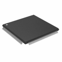
ADSP-21262SKSTZ200 Analog Devices Inc, ADSP-21262SKSTZ200 Datasheet - Page 23

ADSP-21262SKSTZ200
Manufacturer Part Number
ADSP-21262SKSTZ200
Description
IC DSP CONTROLLER 32BIT 144-LQFP
Manufacturer
Analog Devices Inc
Series
SHARC®r
Type
Fixed/Floating Pointr
Specifications of ADSP-21262SKSTZ200
Interface
DAI, SPI
Clock Rate
200MHz
Non-volatile Memory
ROM (512 kB)
On-chip Ram
256kB
Voltage - I/o
3.30V
Voltage - Core
1.20V
Operating Temperature
0°C ~ 70°C
Mounting Type
Surface Mount
Package / Case
144-LQFP
No. Of Bits
32 / 40
Frequency
200MHz
Supply Voltage
1.2V
Embedded Interface Type
Host Port, Serial
Supply Voltage Range
1.14V To 1.26V
Operating Temperature Range
0°C To +70°C
Package
144LQFP
Numeric And Arithmetic Format
Floating-Point
Maximum Speed
200 MHz
Ram Size
256 KB
Device Million Instructions Per Second
200 MIPS
Lead Free Status / RoHS Status
Lead free / RoHS Compliant
Other names
ADSP21262SKSTZ200
ADSP21262SKSTZ200
ADSP21262SKSTZ200
Available stocks
Company
Part Number
Manufacturer
Quantity
Price
Company:
Part Number:
ADSP-21262SKSTZ200
Manufacturer:
Analog Devices Inc
Quantity:
10 000
Precision Clock Generator (Direct Pin Routing)
The timing in
SRU is configured such that the precision clock generator
(PCG) takes its inputs directly from the DAI pins (via pin buff-
ers) and sends its outputs directly to the DAI pins. For the other
Table 17. Precision Clock Generator (Direct Pin Routing)
Parameter
Timing Requirements
t
t
t
Switching Characteristics
t
t
t
PCGIW
STRIG
HTRIG
DPCGIO
DTRIG
PCGOW
Table 17
Input Clock Pulse Width
PCG Trigger Setup Before Falling Edge of PCG Input Clock
PCG Trigger Hold After Falling Edge of PCG Input Clock
PCG Output Clock and Frame Sync Active Edge Delay After PCG Input
Clock Falling Edge
PCG Output Clock and Frame Sync Delay After PCG Trigger
Output Clock Pulse Width
PCG_CLKx_O
PCG_TRIGx_I
and
PCG_EXTx_I
PCG_FSx_O
Figure 15
DAI_Pm
(CLKIN)
DAI_Pn
DAI_Py
DAI_Pz
is valid only when the
Figure 15. Precision Clock Generator (Direct Pin Routing)
t
STRIG
Rev. B | Page 23 of 48 | August 2005
t
HTRIG
t
DTRIG
t
DPCGIO
cases where the PCG’s inputs and outputs are not directly
routed to/from DAI pins (via pin buffers) there is no timing
data available. All timing parameters and switching characteris-
tics apply to external DAI pins (DAI_P07 – DAI_P20).
t
PCGIW
Min
20
2
2
2.5
2.5 + 2.5 × t
40
t
PCGOW
PCGOW
Max
10
10 + 2.5 × t
ADSP-21262
PCGOW
Unit
ns
ns
ns
ns
ns
ns


