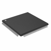
ADSP-21262SKSTZ200 Analog Devices Inc, ADSP-21262SKSTZ200 Datasheet - Page 12

ADSP-21262SKSTZ200
Manufacturer Part Number
ADSP-21262SKSTZ200
Description
IC DSP CONTROLLER 32BIT 144-LQFP
Manufacturer
Analog Devices Inc
Series
SHARC®r
Type
Fixed/Floating Pointr
Specifications of ADSP-21262SKSTZ200
Interface
DAI, SPI
Clock Rate
200MHz
Non-volatile Memory
ROM (512 kB)
On-chip Ram
256kB
Voltage - I/o
3.30V
Voltage - Core
1.20V
Operating Temperature
0°C ~ 70°C
Mounting Type
Surface Mount
Package / Case
144-LQFP
No. Of Bits
32 / 40
Frequency
200MHz
Supply Voltage
1.2V
Embedded Interface Type
Host Port, Serial
Supply Voltage Range
1.14V To 1.26V
Operating Temperature Range
0°C To +70°C
Package
144LQFP
Numeric And Arithmetic Format
Floating-Point
Maximum Speed
200 MHz
Ram Size
256 KB
Device Million Instructions Per Second
200 MIPS
Lead Free Status / RoHS Status
Lead free / RoHS Compliant
Other names
ADSP21262SKSTZ200
ADSP21262SKSTZ200
ADSP21262SKSTZ200
Available stocks
Company
Part Number
Manufacturer
Quantity
Price
Company:
Part Number:
ADSP-21262SKSTZ200
Manufacturer:
Analog Devices Inc
Quantity:
10 000
ADSP-21262
Table 2. Pin Descriptions (Continued)
Pin
DAI_P20–1
SPICLK
SPIDS
MOSI
MISO
BOOTCFG1–0
Type
I/O/T
I/O
I
I/O (O/D)
I/O (O/D)
I
State During and
After Reset
Three-state with
programmable
pull-up
pull-up enabled
Input only
pull-up enabled
pull-up enabled
Input only
Three-state with
Three-state with
Three-state with
Rev. B | Page 12 of 48 | August 2005
Function
Digital Applications Interface Pins. These pins provide the physical interface to
the SRU. The SRU configuration registers define the combination of on-chip
peripheral inputs or outputs connected to the pin and to the pin’s output enable.
The configuration registers of these peripherals then determine the exact behavior
of the pin. Any input or output signal present in the SRU may be routed to any of
these pins. The SRU provides the connection from the serial ports, input data port,
precision clock generators, and timers to the DAI_P20–1 pins. These pins have
internal 22.5 kΩ pull-up resistors which are enabled on reset. These pull-ups can be
disabled in the DAI_PIN_PULLUP register.
Serial Peripheral Interface Clock Signal. Driven by the master, this signal controls
the rate at which data is transferred. The master can transmit data at a variety of
baud rates. SPICLK cycles once for each bit transmitted. SPICLK is a gated clock that
is active during data transfers, only for the length of the transferred word. Slave
devices ignore the serial clock if the slave select input is driven inactive (HIGH).
SPICLK is used to shift out and shift in the data driven on the MISO and MOSI lines.
The data is always shifted out on one clock edge and sampled on the opposite edge
of the clock. Clock polarity and clock phase relative to data are programmable into
the SPICTL control register and define the transfer format. SPICLK has a 22.5 kΩ
internal pull-up resistor. If SPI master boot mode is selected, MOSI and SPICLK pins
are driven during reset. These pins are not three-stated during reset in SPI master
boot mode.
Serial Peripheral Interface Slave Device Select. An active low signal used to select
the DSP as an SPI slave device. This input signal behaves like a chip select, and is
provided by the master device for the slave devices. In multimaster mode the DSP’s
SPIDS signal can be driven by a slave device to signal to the DSP (as SPI master) that
an error has occurred, as some other device is also trying to be the master device.
If asserted low when the device is in master mode, it is considered a multimaster
error. For a single master, multiple-slave configuration where flag pins are used, this
pin must be tied or pulled high to V
ADSP-21262 SPI interaction, any of the master ADSP-21262’s flag pins can be used
to drive the SPIDS signal on the ADSP-21262 SPI slave device.
SPI Master Out Slave In. If the ADSP-21262 is configured as a master, the MOSI pin
becomes a data transmit (output) pin, transmitting output data. If the ADSP-21262
is configured as a slave, the MOSI pin becomes a data receive (input) pin, receiving
input data. In an ADSP-21262 SPI interconnection, the data is shifted out from the
MOSI output pin of the master and shifted into the MOSI input(s) of the slave(s).
MOSI has a 22.5 kΩ internal pull-up resistor. If SPI master boot mode is selected,
MOSI and SPICLK pins are driven during reset. These pins are not three-stated during
reset in SPI master boot mode.
SPI Master In Slave Out. If the ADSP-21262 is configured as a master, the MISO pin
becomes a data receive (input) pin, receiving input data. If the ADSP-21262 is
configured as a slave, the MISO pin becomes a data transmit (output) pin, trans-
mitting output data. In an ADSP-21262 SPI interconnection, the data is shifted out
from the MISO output pin of the slave and shifted into the MISO input pin of the
master. MISO has a 22.5 kΩ internal pull-up resistor. MISO can be configured as O/D
by setting the OPD bit in the SPICTL register.
Note: Only one slave is allowed to transmit data at any given time. To enable broadcast
transmission to multiple SPI slaves, the DSP’s MISO pin may be disabled by setting
(=1) Bit 5 (DMISO) of the SPICTL register.
Boot Configuration Select. Selects the boot mode for the DSP. The BOOTCFG pins
must be valid before reset is asserted. See
the boot modes.
DDEXT
on the master device. For ADSP-21262 to
Table 4 on Page 14
for a description of


