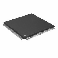
ADSP-BF532SBSTZ400 Analog Devices Inc, ADSP-BF532SBSTZ400 Datasheet - Page 30

ADSP-BF532SBSTZ400
Manufacturer Part Number
ADSP-BF532SBSTZ400
Description
IC DSP CTLR 16BIT 400MHZ 176LQFP
Manufacturer
Analog Devices Inc
Series
Blackfin®r
Type
Fixed Pointr
Datasheet
1.ADSP-BF531SBSTZ400.pdf
(12 pages)
Specifications of ADSP-BF532SBSTZ400
Interface
SPI, SSP, UART
Clock Rate
400MHz
Non-volatile Memory
ROM (1 kB)
On-chip Ram
84kB
Voltage - I/o
1.8V, 2.5V, 3.3V
Voltage - Core
1.20V
Operating Temperature
-40°C ~ 85°C
Mounting Type
Surface Mount
Package / Case
176-LQFP
No. Of Bits
16 Bit
Frequency
400MHz
Supply Voltage
1.2V
Embedded Interface Type
PPI, SPI, UART
No. Of I/o's
16
Supply Voltage Range
0.8V To 1.45V, 1.75V To 3.6V
Lead Free Status / RoHS Status
Lead free / RoHS Compliant
For Use With
ADZS-BF533-EZLITE - KIT W/BOARD EVAL FOR ADSP-BF533
Lead Free Status / RoHS Status
Lead free / RoHS Compliant, Lead free / RoHS Compliant
Available stocks
Company
Part Number
Manufacturer
Quantity
Price
Company:
Part Number:
ADSP-BF532SBSTZ400
Manufacturer:
TOSHIBA
Quantity:
101
Company:
Part Number:
ADSP-BF532SBSTZ400
Manufacturer:
Analog Devices Inc
Quantity:
10 000
Part Number:
ADSP-BF532SBSTZ400
Manufacturer:
ADI/亚德诺
Quantity:
20 000
ADSP-BF531/BF532/BF533
51.
52.
53.
DESCRIPTION:
Heavy I/O activity can cause VDDint to decrease. The reference voltage, which is used to create the set point for the loop, is decreased by
the supply noise. The voltage may drop to a level that is lower than the minimum required to meet your application's frequency of
operations. The VDDint value returns to the programmed value once high I/O activity is halted.
WORKAROUND:
This issue does not occur when an external regulator is used. To determine if the problem exists in your application, you should monitor
the VDDint waveform under the following conditions/setup:
• Apply the maximum VDDext based on the tolerance of VDDext supply.
• Run the application in a steady state (non-startup) condition.
• Connect an oscilloscope with minimum ground and signal loops to VDDint.
• Set the oscilloscope to trigger on a VDDint value that is 5% lower than the programmed value.
The following items can mitigate this issue:
• Lower the I/O activity by reducing SCLK frequency, if possible.
• Increase the programmed value of the voltage regulator by an amount (in multiples of 50mV) closest to the observed decrease.
• Ensure adequate bypassing on VDDext.
APPLIES TO REVISION(S):
0.3, 0.4
DESCRIPTION:
If the internal voltage regulator has been programmed to a voltage level that is different from the default, noise on the voltage regulator
circuit can cause it to spontaneously reset to the default value of 1.2V.
Note that the VLEV bit-field in the VR_CTL register is not affected, so this condition cannot be detected by reading the value of the
register.
WORKAROUND:
None
APPLIES TO REVISION(S):
0.3
DESCRIPTION:
Data can become corrupted if data cache is enabled in write through mode and the AOW bit of the DCPLB is not set and Vddint is 0.9V or
less.
WORKAROUND:
When Vddint <= 0.9V, either operate data cache in write back mode or set the AOW bit of the DCPLB when operating in write through
mode. When Vddint is greater than 0.9V, the errata does not exist.
APPLIES TO REVISION(S):
0.3, 0.4, 0.5, 0.6
05000270 - High I/O Activity Causes Output Voltage of Internal Voltage Regulator (Vddint) to Decrease:
05000271 - Spontaneous Reset of Internal Voltage Regulator:
05000272 - Certain Data Cache Writethrough Modes Fail for Vddint <= 0.9V:
NR003532D | Page 30 of 45 | July 2008
Silicon Anomaly List


