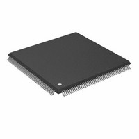
ADSP-BF532SBSTZ400 Analog Devices Inc, ADSP-BF532SBSTZ400 Datasheet - Page 10

ADSP-BF532SBSTZ400
Manufacturer Part Number
ADSP-BF532SBSTZ400
Description
IC DSP CTLR 16BIT 400MHZ 176LQFP
Manufacturer
Analog Devices Inc
Series
Blackfin®r
Type
Fixed Pointr
Datasheet
1.ADSP-BF531SBSTZ400.pdf
(12 pages)
Specifications of ADSP-BF532SBSTZ400
Interface
SPI, SSP, UART
Clock Rate
400MHz
Non-volatile Memory
ROM (1 kB)
On-chip Ram
84kB
Voltage - I/o
1.8V, 2.5V, 3.3V
Voltage - Core
1.20V
Operating Temperature
-40°C ~ 85°C
Mounting Type
Surface Mount
Package / Case
176-LQFP
No. Of Bits
16 Bit
Frequency
400MHz
Supply Voltage
1.2V
Embedded Interface Type
PPI, SPI, UART
No. Of I/o's
16
Supply Voltage Range
0.8V To 1.45V, 1.75V To 3.6V
Lead Free Status / RoHS Status
Lead free / RoHS Compliant
For Use With
ADZS-BF533-EZLITE - KIT W/BOARD EVAL FOR ADSP-BF533
Lead Free Status / RoHS Status
Lead free / RoHS Compliant, Lead free / RoHS Compliant
Available stocks
Company
Part Number
Manufacturer
Quantity
Price
Company:
Part Number:
ADSP-BF532SBSTZ400
Manufacturer:
TOSHIBA
Quantity:
101
Company:
Part Number:
ADSP-BF532SBSTZ400
Manufacturer:
Analog Devices Inc
Quantity:
10 000
Part Number:
ADSP-BF532SBSTZ400
Manufacturer:
ADI/亚德诺
Quantity:
20 000
ADSP-BF531/BF532/BF533
13.
14.
DESCRIPTION:
Consider the following scenario:
In this case, an erroneous interrupt will occur, even though no edge was physically present at the input. This will also occur at any
subsequent writes of a 1 to this bit of the polarity register. If the polarity register is reset to 0, no interrupt is generated, as expected.
In the opposite case, with the external pin level equal to 1, the erroneous interrupt is generated when the polarity bit is changed from 1 to
0 (and any subsequent writes of a 1 to this bit of the polarity register), and not when changed from 0 to 1.
In the case of multiple I/O pins configured as edge-sensitive interrupts, ANY change to the polarity register will affect all those I/O pins in
the above manner. The workaround in this case needs to be applied to all of those pins.
Similar considerations apply to the input enable register. Changing this setting while edge-sensitive interrupts are enabled will also cause
unwanted interrupts.
WORKAROUND:
Prior to changing the polarity (and/or input enable) register(s), disable the interrupts (i.e., by clearing the PFA or PFB IMASK bit), change
the register setting, clear the interrupt request as you normally would (write to the data or clear registers), and then re-enable the
interrupt again.
APPLIES TO REVISION(S):
0.3
DESCRIPTION:
When using internal SPORT clocks or external SPORT clocks with falling edge selected (SPORTx_TCR1:TCKE, SPORTx_RCR1:RCKE), if the
SPORT is disabled and then subsequently re-enabled, there is a possibility of corrupting the first word transmitted or received.
WORKAROUND:
For internal SPORT clocks:
After disabling the SPORT, write bit 1 of the SPORT configuration 1 register (SPORTx_TCR1:ITCLK, SPORTx_RCR1:IRCLK) to 0. This will
switch the SPORT clock to external, allowing the SPORT to be fully reset.
For external SPORT clocks with falling edge selected:
After disabling the SPORT, write bit 14 of the SPORT configuration 1 register (SPORTx_TCR1:TCKE, SPORTx_RCR1:RCKE) to 0. This will allow
the SPORT to be fully reset.
APPLIES TO REVISION(S):
0.3
05000193 - False I/O Pin Interrupts on Edge-Sensitive Inputs When Polarity Setting Is Changed:
05000194 - Restarting SPORT in Specific Modes May Cause Data Corruption:
1) Pins are configured as edge-sensitive inputs.
2) The interrupt occurs on the rising edge.
3) Input level is constant and 0.
4) Change the polarity setting to set the interrupt to occur on the falling edge instead.
NR003532D | Page 10 of 45 | July 2008
Silicon Anomaly List


