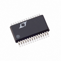
LTC2408CG Linear Technology, LTC2408CG Datasheet - Page 30

LTC2408CG
Manufacturer Part Number
LTC2408CG
Description
IC A/D CONV 24BIT 8-CHAN 28-SSOP
Manufacturer
Linear Technology
Datasheet
1.LTC2408CGPBF.pdf
(36 pages)
Specifications of LTC2408CG
Number Of Bits
24
Sampling Rate (per Second)
7.5
Data Interface
MICROWIRE™, Serial, SPI™
Number Of Converters
1
Power Dissipation (max)
1mW
Voltage Supply Source
Single Supply
Operating Temperature
0°C ~ 70°C
Mounting Type
Surface Mount
Package / Case
28-SSOP (0.200", 5.30mm Width)
Lead Free Status / RoHS Status
Contains lead / RoHS non-compliant
Available stocks
Company
Part Number
Manufacturer
Quantity
Price
Company:
Part Number:
LTC2408CG
Manufacturer:
LINEAR
Quantity:
6
Part Number:
LTC2408CG
Manufacturer:
LT/凌特
Quantity:
20 000
Part Number:
LTC2408CG#PBF
Manufacturer:
LINEAR/凌特
Quantity:
20 000
Part Number:
LTC2408CG#TRPBF
Manufacturer:
LINEAR/凌特
Quantity:
20 000
APPLICATIONS
LTC2404/LTC2408
DIN1
DIN2
DIN3
DIN4
MUX
*
***************************************
* Start GETDATA Routine
***************************************
*
*
INIT1
*
*
* DDRD’s bit 5 is a 1 so that port D’s SS* pin is a general output
*
*
*
*
GETDATA PSHX
*
*
*******************************
* The next routine sends data to the *
* LTC2408 an sets its MUX channel *
*******************************
*
*
WAITMUX LDAA
*
***************************************
* Enable the LTC2408
***************************************
*
*
*
***************************************
* The next short loop waits for the
* LTC2408’s conversion to finish before
* starting the SPI data transfer
***************************************
*
CONVEND LDAA
*
*
*
*
30
EQU
EQU
EQU
EQU
EQU
ORG
LDS
LDAA
STAA
LDAA
STAA
LDAA
STAA
PSHY
PSHA
LDX
LDY
LDAA
ORAA
STAA
BCLR
ANDA
BNE
$00
$01
$02
$03
$04
$C000
$CFFF
#$2F
PORTD
#$38
DDRD
#$50
SPCR
#$0
#$1000
$MUX
#$08
SPDR
SPSR
BPL
PORTD,Y %00100000 This sets the SS* output bit to a logic
PORTD
#%00000100
CONVEND
U
This memory location holds the LTC2408’s bits 31 - 24
This memory location holds the LTC2408’s bits 23 - 16
This memory location holds the LTC2408’s bits 15 - 08
This memory location holds the LTC2408’s bits 07 - 00
This memory location holds the MUX address data
Program start location
Top of C page RAM, beginning location of stack
-,-,1,0;1,1,1,1
-, -, SS*-Hi, SCK-Lo, MOSI-Hi, MISO-Hi, X, X
Keeps SS* a logic high when DDRD, bit 5 is set
-,-,1,1;1,0,0,0
SS* , SCK, MOSI are configured as Outputs
MISO, TxD, RxD are configured as Inputs
The SPI is configured as Master, CPHA = 0, CPOL = 0
and the clock rate is E/2
(This assumes an E-Clock frequency of 4MHz. For higher
E-Clock frequencies, change the above value of $50 to a
value that ensures the SCK frequency is 2MHz or less.)
The X register is used as a pointer to the memory
locations that hold the conversion data
Retrieve MUX address
Set the MUX’s ENABLE bit
Transfer Accum. A contents to SPI register to initiate
serial transfer
Get SPI transfer status
WAITMUX If the transfer is not finished, read status
INFORMATION
U
*
*
low, selecting the LTC2408
*
*
*
Retrieve the contents of port D
Look at bit 2
Bit 2 = Hi; the LTC2408’s conversion is not
complete
Bit 2 = Lo; the LTC2408’s conversion is complete
Branch to the loop’s beginning while bit 2 remains
high
W
U


