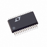
LTC2408CG Linear Technology, LTC2408CG Datasheet - Page 13

LTC2408CG
Manufacturer Part Number
LTC2408CG
Description
IC A/D CONV 24BIT 8-CHAN 28-SSOP
Manufacturer
Linear Technology
Datasheet
1.LTC2408CGPBF.pdf
(36 pages)
Specifications of LTC2408CG
Number Of Bits
24
Sampling Rate (per Second)
7.5
Data Interface
MICROWIRE™, Serial, SPI™
Number Of Converters
1
Power Dissipation (max)
1mW
Voltage Supply Source
Single Supply
Operating Temperature
0°C ~ 70°C
Mounting Type
Surface Mount
Package / Case
28-SSOP (0.200", 5.30mm Width)
Lead Free Status / RoHS Status
Contains lead / RoHS non-compliant
Available stocks
Company
Part Number
Manufacturer
Quantity
Price
Company:
Part Number:
LTC2408CG
Manufacturer:
LINEAR
Quantity:
6
Part Number:
LTC2408CG
Manufacturer:
LT/凌特
Quantity:
20 000
Part Number:
LTC2408CG#PBF
Manufacturer:
LINEAR/凌特
Quantity:
20 000
Part Number:
LTC2408CG#TRPBF
Manufacturer:
LINEAR/凌特
Quantity:
20 000
APPLICATIONS
Bit 31 (first output bit) is the end of conversion (EOC)
indicator. This bit is available at the SDO pin during the
conversion and sleep states whenever the CSADC pin is
LOW. This bit is HIGH during the conversion and goes
LOW when the conversion is complete.
Bit 30 (second output bit) is a dummy bit (DMY) and is
always LOW.
Bit 29 (third output bit) is the conversion result sign indi-
cator (SIG). If V
bit is LOW. The sign bit changes state during the zero code.
Bit 28 (forth output bit) is the extended input range (EXR)
indicator. If the input is within the normal input range
0 V
normal input range, V
The function of these bits is summarized in Table 1.
Table 1. LTC2404/LTC2408 Status Bits
Input Range
V
0 < V
V
V
Bit 27 (fifth output bit) is the most significant bit (MSB).
Bits 27-4 are the 24-bit conversion result MSB first.
Bit 4 is the least significant bit (LSB).
IN
IN
IN
> V
= 0
< 0
IN
IN
REF
+
/0
CSMUX/CSADC
V
–
REF
V
SCK/CLK
REF
SDO
, this bit is LOW. If the input is outside the
D
IN
IN
Bit 31
is >0, this bit is HIGH. If V
EOC
EN
U
0
0
0
0
IN
> V
D2
INFORMATION
U
REF
Hi-Z
Bit 30
D1
DMY
or V
0
0
0
0
IN
D0
W
< 0, this bit is HIGH.
Bit 29
Figure 3. Typical Data Input/Output Timing
SIG
1/0
1
1
0
EOC
BIT 31
IN
U
is <0, this
BIT 30
“0”
Bit 28
EXR
1
0
0
1
SIG
EXT
Bits 3-0 are sub LSBs below the 24-bit level. Bits 3-0 may
be included in averaging or discarded without loss of
resolution.
Data is shifted out of the SDO pin under control of the serial
clock (SCK), see Figure 3. Whenever CSADC is HIGH, SDO
remains high impedance and any SCK clock pulses are
ignored by the internal data out shift register.
In order to shift the conversion result out of the device,
CSADC must first be driven LOW. EOC is seen at the SDO
pin of the device once CSADC is pulled LOW. EOC changes
in real time from HIGH to LOW at the completion of a
conversion. This signal may be used as an interrupt for an
external microcontroller. Bit 31 (EOC) can be captured on
the first rising edge of SCK. Bit 30 is shifted out of the
device on the first falling edge of SCK. The final data bit
(Bit 0) is shifted out on the falling edge of the 31st SCK and
may be latched on the rising edge of the 32nd SCK pulse.
On the falling edge of the 32nd SCK pulse, SDO goes HIGH
indicating a new conversion cycle has been initiated. This
bit serves as EOC (Bit 31) for the next conversion cycle.
Table 2 summarizes the output data format.
As long as the voltage on the V
the – 0.3V to (V
range, a conversion result is generated for any input value
from – 0.125 • V
greater than 1.125 • V
to the value corresponding to 1.125 • V
voltages below – 0.125 • V
clamped to the value corresponding to – 0.125 • V
MSB
DON’T CARE
CC
LSB
BIT 0
REF
+ 0.3V) absolute maximum operating
REF
to 1.125 • V
LTC2404/LTC2408
, the conversion result is clamped
REF
IN
, the conversion result is
pin is maintained within
REF
t
Hi-Z
CONV
. For input voltages
REF
. For input
24048 F03
13
REF
.


