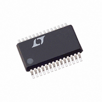
LTC2408CG Linear Technology, LTC2408CG Datasheet - Page 23

LTC2408CG
Manufacturer Part Number
LTC2408CG
Description
IC A/D CONV 24BIT 8-CHAN 28-SSOP
Manufacturer
Linear Technology
Datasheet
1.LTC2408CGPBF.pdf
(36 pages)
Specifications of LTC2408CG
Number Of Bits
24
Sampling Rate (per Second)
7.5
Data Interface
MICROWIRE™, Serial, SPI™
Number Of Converters
1
Power Dissipation (max)
1mW
Voltage Supply Source
Single Supply
Operating Temperature
0°C ~ 70°C
Mounting Type
Surface Mount
Package / Case
28-SSOP (0.200", 5.30mm Width)
Lead Free Status / RoHS Status
Contains lead / RoHS non-compliant
Available stocks
Company
Part Number
Manufacturer
Quantity
Price
Company:
Part Number:
LTC2408CG
Manufacturer:
LINEAR
Quantity:
6
Part Number:
LTC2408CG
Manufacturer:
LT/凌特
Quantity:
20 000
Part Number:
LTC2408CG#PBF
Manufacturer:
LINEAR/凌特
Quantity:
20 000
Part Number:
LTC2408CG#TRPBF
Manufacturer:
LINEAR/凌特
Quantity:
20 000
power dissipation. A series resistor between 27 and 56
placed near the driver or near the LTC2404/LTC2408 pin
will also eliminate this problem without additional power
dissipation. The actual resistor value depends upon the
trace impedance and connection topology.
Driving the Input and Reference
The analog input and reference of the typical delta-sigma
analog-to-digital converter are applied to a switched ca-
pacitor network. This network consists of capacitors switch-
ing between the analog input (ADCIN), ground and the
reference (V
both ADCIN and V
is shown in Figure 12.
The key to understanding the effects of this dynamic input
current is based on a simple first order RC time constant
model. Using the internal oscillator, the internal switched
capacitor network of the LTC2404/LTC2408 is clocked at
153,600Hz corresponding to a 6.5 s sampling period.
Fourteen time constants are required each time a capacitor
is switched in order to achieve 1ppm settling accuracy.
Therefore, the equivalent time constant at V
should be less than 6.5 s/14 = 460ns in order to achieve
1ppm accuracy.
Input Current (V
If complete settling occurs on the input, conversion re-
sults will be uneffected by the dynamic input current. If the
settling is incomplete, it does not degrade the linearity
APPLICATIONS
REF
). The result is small current spikes seen at
SELECTED
CHANNEL
f
f
EXTERNAL OSCILLATOR: 2.56kHz f 307.2kHz
IN
OUT
OUT
CHX
REF
)
= 50Hz, INTERNAL OSCILLATOR: f = 128kHz
= 60Hz, INTERNAL OSCILLATOR: f = 153.6kHz
U
. A simplified input equivalent circuit
I
I
IN(MUX)
IN(MUX)
INFORMATION
U
MUXV
(PIN 8)
CC
Figure 12. LTC2404/LTC2408 Equivalent Analog Input Circuit
R
75
SW
W
MUXOUT
IN
U
and V
ADCIN
GND
I
DC
REF
V
REF
I
I
IN(LEAK)
IN(LEAK)
I
I
performance of the device. It simply results in an offset/
full-scale shift, see Figure 13. To simplify the analysis of
input dynamic current, two separate cases are assumed:
large capacitance at V
tance at V
If the total capacitance at V
(< 0.01 F), relatively large external source resistances (up
to 20k for 20pF parasitic capacitance) can be tolerated
without any offset/full-scale error. Figures 15 and 16 show
a family of offset and full-scale error curves for various
REF
REF
ADCV
ADCV
(PIN 2)
(PIN 2)
TUE
CC
CC
R
R
R
5k
5k
5k
SOURCE
SW
SW
SW
0
SIGNAL
INTPUT
IN
Figure 14. An RC Network at CH0 to CH7
(C
Figure 13. Offset/Full-Scale Shift
IN
< 0.01 F).
R
24048 F12
I
SOURCE
DC
= 0.25(V
AVERAGE INPUT CURRENT:
IN
LTC2404/LTC2408
(C
IN
IN
V
C
– 0.5 • V
REF
V
IN
> 0.01 F) and small capaci-
IN
IN
C
10pF (TYP)
/2
EQ
(see Figure 14) is small
REF
C
) • f • C
PAR
20pF
EQ
CH0 TO
CH7
LTC2404/
LTC2408
24048 F14
24048 F13
V
REF
23


