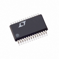
LTC2408CG Linear Technology, LTC2408CG Datasheet - Page 16

LTC2408CG
Manufacturer Part Number
LTC2408CG
Description
IC A/D CONV 24BIT 8-CHAN 28-SSOP
Manufacturer
Linear Technology
Datasheet
1.LTC2408CGPBF.pdf
(36 pages)
Specifications of LTC2408CG
Number Of Bits
24
Sampling Rate (per Second)
7.5
Data Interface
MICROWIRE™, Serial, SPI™
Number Of Converters
1
Power Dissipation (max)
1mW
Voltage Supply Source
Single Supply
Operating Temperature
0°C ~ 70°C
Mounting Type
Surface Mount
Package / Case
28-SSOP (0.200", 5.30mm Width)
Lead Free Status / RoHS Status
Contains lead / RoHS non-compliant
Available stocks
Company
Part Number
Manufacturer
Quantity
Price
Company:
Part Number:
LTC2408CG
Manufacturer:
LINEAR
Quantity:
6
Part Number:
LTC2408CG
Manufacturer:
LT/凌特
Quantity:
20 000
Part Number:
LTC2408CG#PBF
Manufacturer:
LINEAR/凌特
Quantity:
20 000
Part Number:
LTC2408CG#TRPBF
Manufacturer:
LINEAR/凌特
Quantity:
20 000
APPLICATIONS
LTC2404/LTC2408
Using an External Clock for Faster Conversion Times
The conversion time of the LTC2404/LTC2408 is deter-
mined by the conditions on the F
to GND for 60Hz rejection, the conversion time is 133 s.
If F
an externally supplied frequency of f
version time is:
The resulting frequency rejection is:
The maximum output word rate is:
16
O
t
Notch Frequency = 8/t
OWR
CONV
is connected to V
Figure 6. Resolution vs Maximum Output Rate
= 20480/f
20
18
16
14
10
24
22
12
20
18
16
14
10
Figure 5. INL vs Maximum Output Rate
24
22
12
t
8
8
CONVERT
0
0
*RESOLUTION =
5
5
V
CC
10
10
MAXIMUM OUTPUT RATE (Hz)
MAXIMUM OUTPUT RATE (Hz)
EOSC
= V
U
T
15 20 25
15 20 25
A
CC
REF
= 90 C
, the conversion time is 160 s. For
1
t
= 3V
(kHz)
DATAOUTPUT
LOG(V
INFORMATION
CONV
U
30 35 40 45 50 55
30 35 40 45 50 55
T
REF
V
V
F
(20480 MAXIMUM
OUTPUT RATE)
A
F
(20480 MAXIMUM
OUTPUT RATE)
LOG (2)
0
CC
REF
O
= 25 C
/RMS NOISE)
= EXTERNAL
= EXTERNAL
V
= 5V
CC
T
T
O
= 5V
A
A
= V
pin. If F
= 25 C
= 90 C
W
REF
EOSC
in Hz
24048 G27
24048 G28
= 5V
(kHz), the con-
O
60
60
is connected
U
The DC specifications are guaranteed for f
maximum of 307.2kHz, resulting in a maximum output
word rate of approximately 15Hz. However, for faster rates
at reduced performance, frequencies up to 1.22MHz can
be used on the F
Resolution vs Output Rate.
SERIAL INTERFACE
The LTC2404/LTC2408 transmit the conversion results,
program the channel selection, and receive the start of
conversion command through a synchronous 4-wire in-
terface (SCK = CLK, CSADC = CSMUX). During the conver-
sion and sleep states, this interface can be used to assess
the converter status. While in the sleep state this interface
may be used to program an input channel. During the data
output state it is used to read the conversion result.
ADC Serial Clock Input/Output (SCK)
The serial clock signal present on SCK (Pin 25) is used to
synchronize the data transfer. Each bit of data is shifted out
the SDO pin on the falling edge of the serial clock.
In the Internal SCK mode of operation, the SCK pin is an
output and the LTC2404/LTC2408 creates its own serial
clock by dividing the internal conversion clock by 8. In the
External SCK mode of operation, the SCK pin is used as
input. The internal or external SCK mode is selected on
power-up and then reselected every time a HIGH-to-LOW
transition is detected at the CSADC pin. If SCK is HIGH or
floating at power-up or during this transition, the converter
enters the internal SCK mode. If SCK is LOW at power-up
or during this transition, the converter enters the external
SCK mode.
Multiplexer Serial Input Clock (CLK)
Generally, this pin is externally tied to SCK for 4-wire op-
eration. On the rising edge of CLK (Pin 19) with CSMUX held
HIGH, data is serially shifted into the multiplexer. If CSMUX
is LOW the CLK input will be disabled and the channel
selection unchanged.
Serial Data Output (SDO)
The serial data output pin, SDO (Pin 24), drives the serial
data during the data output state. In addition, the SDO pin
O
pin. Figures 5 and 6 show the INL and
EOSC
up to a


