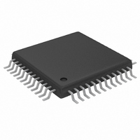
MAX1198ECM+D Maxim Integrated Products, MAX1198ECM+D Datasheet - Page 18

MAX1198ECM+D
Manufacturer Part Number
MAX1198ECM+D
Description
IC ADC 8BIT 100MSPS DUAL 48-TQFP
Manufacturer
Maxim Integrated Products
Datasheet
1.MAX1198ECMD.pdf
(22 pages)
Specifications of MAX1198ECM+D
Number Of Bits
8
Sampling Rate (per Second)
100M
Data Interface
Parallel
Number Of Converters
2
Power Dissipation (max)
314mW
Voltage Supply Source
Single Supply
Operating Temperature
-40°C ~ 85°C
Mounting Type
Surface Mount
Package / Case
48-TQFP Exposed Pad, 48-eTQFP, 48-HTQFP, 48-VQFP
Conversion Rate
100 MSPs
Resolution
8 bit
Snr
48.5 dB
Voltage Reference
2.048 V
Supply Voltage (max)
3.6 V
Supply Voltage (min)
2.7 V
Maximum Power Dissipation
1000 mW
Maximum Operating Temperature
+ 85 C
Mounting Style
SMD/SMT
Input Voltage
3.3 V
Minimum Operating Temperature
- 40 C
Lead Free Status / RoHS Status
Lead free / RoHS Compliant
Figure 9. External Unbuffered Reference Drive with MAX4252 and MAX6066
Dual, 8-Bit, 100Msps, 3.3V, Low-Power ADC
with Internal Reference and Parallel Outputs
shifted with respect to the in-phase component. At the
receiver, the QAM signal is divided down into its I and
Q components, essentially representing the modulation
process reversed.
process performed in the analog domain, using the
dual matched 3.3V, 8-bit ADC MAX1198 and the
MAX2451 quadrature demodulator to recover and
digitize the I and Q baseband signals. Before being
digitized by the MAX1198, the mixed down-signal com-
ponents may be filtered by matched analog filters, such
as Nyquist or pulse-shaping filters, which remove
unwanted images from the mixing process, thereby
enhancing the overall signal-to-noise (SNR) perfor-
mance and minimizing intersymbol interference.
18
MAX4254 POWER-SUPPLY
BYPASSING. PLACE CAPACITOR
AS CLOSE AS POSSIBLE TO
THE OP AMP.
NOTE: ONE FRONT-END REFERENCE CIRCUIT DESIGN MAY BE USED WITH UP TO 32 ADCs.
3.3V
MAX6066
______________________________________________________________________________________
1
3
0.1µF
3.3V
2
21.5kΩ
0.1µF
Figure 10 displays the demodulation
1µF
21.5kΩ
21.5kΩ
21.5kΩ
21.5kΩ
2.0V
1.5V
1.0V
10
3
2
5
6
9
4
4
4
11
11
11
1/4 MAX4252
1/4 MAX4252
1/4 MAX4252
3.3V
3.3V
3.3V
1
7
8
10µF
6V
10µF
6V
10µF
6V
1.47kΩ
1.47kΩ
1.47kΩ
47Ω
47Ω
47Ω
1.0V AT -8mA
2.0V AT 8mA
1.5V AT 0mA
The MAX1198 requires high-speed board layout design
techniques. Locate all bypass capacitors as close to
the device as possible, preferably on the same side as
the ADC, using surface-mount devices for minimum
inductance. Bypass V
two parallel 0.1µF ceramic capacitors and a 2.2µF
bipolar capacitor to GND. Follow the same rules to
bypass the digital supply (OV
boards with separated ground and power planes
produce the highest level of signal integrity. Consider
the use of a split ground plane arranged to match the
330µF
6V
330µF
330µF
6V
6V
0.1µF
0.1µF
N.C.
N.C.
0.1µF
0.1µF
Grounding, Bypassing,
DD
0.1µF
0.1µF
, REFP, REFN, and COM with
and Board Layout
29
31
32
29
31
32
1
2
1
2
DD
REFOUT
REFIN
REFP
REFN
COM
REFOUT
REFIN
REFP
REFN
COM
) to OGND. Multilayer
MAX1198
MAX1198
N = 32
N = 1
0.1µF
2.2µF
10V


