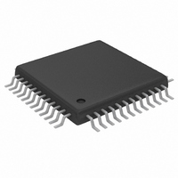
MAX1198ECM+D Maxim Integrated Products, MAX1198ECM+D Datasheet

MAX1198ECM+D
Specifications of MAX1198ECM+D
Related parts for MAX1198ECM+D
MAX1198ECM+D Summary of contents
Page 1
... Set-Top Boxes Ultrasound and Medical Imaging VSAT Terminals Battery-Powered Instrumentation ________________________________________________________________ Maxim Integrated Products For pricing, delivery, and ordering information, please contact Maxim/Dallas Direct! at 1-888-629-4642, or visit Maxim’s website at www.maxim-ic.com. o Single 2.7V to 3.6V Operation o Excellent Dynamic Performance 48.1dB/47.6dB SINAD at f 66dBc/61.5dBc SFDR at f ...
Page 2
Dual, 8-Bit, 100Msps, 3.3V, Low-Power ADC with Internal Reference and Parallel Outputs ABSOLUTE MAXIMUM RATINGS GND ...............................................-0.3V to +3. OGND to GND.......................................................-0.3V to +0.3V INA+, INA-, INB+, INB- to GND ...............................-0. REFIN, ...
Page 3
Dual, 8-Bit, 100Msps, 3.3V, Low-Power ADC with Internal Reference and Parallel Outputs ELECTRICAL CHARACTERISTICS (continued 3.3V 2.5V, 0.1µF and 2.2µF capacitors from REFP, REFN, and COM to GND; REFOUT connected to REFIN through ...
Page 4
Dual, 8-Bit, 100Msps, 3.3V, Low-Power ADC with Internal Reference and Parallel Outputs ELECTRICAL CHARACTERISTICS (continued 3.3V 2.5V, 0.1µF and 2.2µF capacitors from REFP, REFN, and COM to GND; REFOUT connected to REFIN through ...
Page 5
Dual, 8-Bit, 100Msps, 3.3V, Low-Power ADC with Internal Reference and Parallel Outputs ELECTRICAL CHARACTERISTICS (continued 3.3V 2.5V, 0.1µF and 2.2µF capacitors from REFP, REFN, and COM to GND; REFOUT connected to REFIN through ...
Page 6
Dual, 8-Bit, 100Msps, 3.3V, Low-Power ADC with Internal Reference and Parallel Outputs ELECTRICAL CHARACTERISTICS (continued 3.3V 2.5V, 0.1µF and 2.2µF capacitors from REFP, REFN, and COM to GND; REFOUT connected to REFIN through ...
Page 7
Dual, 8-Bit, 100Msps, 3.3V, Low-Power ADC with Internal Reference and Parallel Outputs (V = 3.3V 2.5V 2.048V, differential input at -1dB FS REFIN noted.) FFT PLOT CHA (DIFFERENTIAL INPUT, 8192-POINT DATA RECORD) 0 ...
Page 8
Dual, 8-Bit, 100Msps, 3.3V, Low-Power ADC with Internal Reference and Parallel Outputs (V = 3.3V 2.5V 2.048V, differential input at -1dB FS REFIN noted.) SNR/SINAD, THD/SFDR vs. TEMPERATURE 19.87089082MHz IN ...
Page 9
Dual, 8-Bit, 100Msps, 3.3V, Low-Power ADC with Internal Reference and Parallel Outputs (V = 3.3V 2.5V 2.048V, differential input at -1dB FS REFIN noted.) GAIN ERROR vs. TEMPERATURE, EXTERNAL REFERENCE V = 2.048V ...
Page 10
Dual, 8-Bit, 100Msps, 3.3V, Low-Power ADC with Internal Reference and Parallel Outputs PIN NAME Common-Mode Voltage I/O. Bypass to GND with a ≥0.1µF capacitor. 1 COM Analog Supply Voltage. Bypass to GND with a capacitor combination of 2.2µF in parallel ...
Page 11
Dual, 8-Bit, 100Msps, 3.3V, Low-Power ADC with Internal Reference and Parallel Outputs PIN NAME 42 D5A Three-State Digital Output, Bit 5, Channel A 43 D6A Three-State Digital Output, Bit 6, Channel A 44 D7A Three-State Digital Output, Bit 7 (MSB), ...
Page 12
Dual, 8-Bit, 100Msps, 3.3V, Low-Power ADC with Internal Reference and Parallel Outputs S4a INA+ INA- S4b S4a INB+ INB- S4b Figure 2. MAX1198 T/H Amplifiers are closed. The fully differential circuits sample the input signals onto the two capacitors (C2a ...
Page 13
Dual, 8-Bit, 100Msps, 3.3V, Low-Power ADC with Internal Reference and Parallel Outputs ANALOG INPUT CLOCK INPUT t DO DATA OUTPUT D7A–D0A DATA OUTPUT D7B–D0B Figure 3. System Timing Diagram Match the impedance of INA+ ...
Page 14
Dual, 8-Bit, 100Msps, 3.3V, Low-Power ADC with Internal Reference and Parallel Outputs DISABLE ENABLE OUTPUT HIGH-Z VALID DATA D7A–D0A OUTPUT HIGH-Z VALID DATA D7B–D0B Figure 4. Output Timing Diagram The MAX1198 clock input operates with a voltage ...
Page 15
Dual, 8-Bit, 100Msps, 3.3V, Low-Power ADC with Internal Reference and Parallel Outputs 300Ω 300Ω +5V 0.1µF INPUT MAX4108 0.1µF -5V 300Ω 300Ω 300Ω +5V 300Ω 0.1µF 0.1µF INPUT MAX4108 0.1µF -5V 300Ω 300Ω Figure 5. Typical Application for Single-Ended-to-Differential Conversion ...
Page 16
Dual, 8-Bit, 100Msps, 3.3V, Low-Power ADC with Internal Reference and Parallel Outputs 25Ω 22pF 0.1µ N.C. 2.2µF 0.1µ MINICIRCUITS TT1–6-KK81 25Ω 22pF 25Ω 22pF 0.1µ ...
Page 17
Dual, 8-Bit, 100Msps, 3.3V, Low-Power ADC with Internal Reference and Parallel Outputs 3.3V 0.1µF 0.1µF 1 16.2kΩ 2 MAX6062 1µF 3 10Hz LOWPASS FILTER NOTE: ONE FRONT-END REFERENCE CIRCUIT DESIGN MAY BE USED WITH UP TO 1000 ADCs. Figure 8. ...
Page 18
Dual, 8-Bit, 100Msps, 3.3V, Low-Power ADC with Internal Reference and Parallel Outputs 3.3V 0.1µF 1 2.0V 21.5kΩ 2 MAX6066 3 21.5kΩ 1.5V 1µF 21.5kΩ 3.3V 1.0V 0.1µF 10 21.5kΩ MAX4254 POWER-SUPPLY BYPASSING. PLACE CAPACITOR 21.5kΩ AS CLOSE AS POSSIBLE TO ...
Page 19
Dual, 8-Bit, 100Msps, 3.3V, Low-Power ADC with Internal Reference and Parallel Outputs Figure 10. Typical QAM Application Using the MAX1198 CLK ANALOG INPUT SAMPLED DATA (T/H) TRACK HOLD T/H Figure 11. T/H Aperture Timing physical location ...
Page 20
Dual, 8-Bit, 100Msps, 3.3V, Low-Power ADC with Internal Reference and Parallel Outputs In reality, there are other noise sources besides quanti- zation noise: thermal noise, reference noise, clock jitter, etc. SNR is computed by taking the ratio of the RMS ...
Page 21
Dual, 8-Bit, 100Msps, 3.3V, Low-Power ADC with Internal Reference and Parallel Outputs V DD GND INA+ T/H INA- CLK INB+ T/H INB- REFOUT Pin-Compatible Upgrades (Sampling Speed and Resolution) 8-BIT PART 10-BIT PART MAX1195 MAX1183 MAX1197 MAX1182 MAX1198 MAX1180 MAX1196* ...
Page 22
... Maxim cannot assume responsibility for use of any circuitry other than circuitry entirely embodied in a Maxim product. No circuit patent licenses are implied. Maxim reserves the right to change the circuitry and specifications without notice at any time. 22 ____________________Maxim Integrated Products, 120 San Gabriel Drive, Sunnyvale, CA 94086 408-737-7600 © 2002 Maxim Integrated Products Printed USA is a registered trademark of Maxim Integrated Products ...


