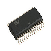
CY7C65113-SXC Cypress Semiconductor Corp, CY7C65113-SXC Datasheet - Page 43

CY7C65113-SXC
Manufacturer Part Number
CY7C65113-SXC
Description
Manufacturer
Cypress Semiconductor Corp
Datasheet
1.CY7C65113-SXC.pdf
(49 pages)
Specifications of CY7C65113-SXC
Operating Temperature (max)
70C
Operating Temperature (min)
0C
Operating Temperature Classification
Commercial
Package Type
SOIC
Mounting
Surface Mount
Lead Free Status / RoHS Status
Compliant
Available stocks
Company
Part Number
Manufacturer
Quantity
Price
Company:
Part Number:
CY7C65113-SXC
Manufacturer:
CYPRESS
Quantity:
770
Part Number:
CY7C65113-SXC
Manufacturer:
CYPRESS/赛普拉斯
Quantity:
20 000
Document #: 38-08002 Rev. *D
19.0
Note:
7.
B: Read and Write; W: Write; R: Read.
Address
0x00
0x01
0x02
0x03
0x04
0x05
0x08
0x09
0x10
0x12
0x13
0x14
0x15
0x16
0x1F
0x20
0x21
0x24
0x25
0x28
0x29
0x40
0x41
0x42
0x43
0x44
0x11
Register Summary
Port 0 Data
Port 1 Data
Port 2 Data
Port 3 Data
Port 0 Interrupt Enable
Port 1 Interrupt Enable
GPIO Configuration
HAPI/I
USB Device Address A
EP A0 Counter
Register
EP A0 Mode Register
EP A1 Counter
Register
EP A1 Mode Register
EP A2 Counter
Register
EP A2 Mode Register
USB Status and Control
Global Interrupt Enable
Endpoint Interrupt
Enable
Timer (LSB)
Timer (MSB)
I
I
USB Device Address B
EP B0 Counter Register
EP B0 Mode Register
EP B1 Counter Register
EP B1 Mode Register
2
2
C Control and Status
C Data
Register Name
2
C Configuration
I
2
Timer Bit 7
Endpoint 0
Address A
Endpoint0
Address B
I
Reserved
Received
Reserved
Reserved
Reserved
Received
Endpoint
P0.7 Intr
P1.7 Intr
C Position
Data 0/1
Data 0/1
Data 0/1
2
Data 0/1
Data 0/1
SETUP
SETUP
Enable
Enable
Device
Enable
Toggle
Toggle
STALL
Toggle
STALL
Device
Enable
Toggle
Toggle
STALL
MSTR
C Data 7
Mode
Bit 7
P0.7
P1.7
P2.7
P3.7
Size
Timer Bit 6
Address A
Address B
Endpoint 0
Data Valid
Endpoint0
Data Valid
Data Valid
Data Valid
Data Valid
Reserved
Reserved
Reserved
Reserved
Continue/
I
Received
Received
Endpoint
P0.6 Intr
P1.6 Intr
Interrupt
2
Enable
Enable
Device
Enable
Device
C Data 6
Mode
Busy
Bit 6
P0.6
P1.6
P2.6
P3.6
Bit 6
Bit 6
I
IN
IN
2
-
-
-
C
Byte Count
Byte Count
Byte Count
Byte Count
Byte Count
Timer Bit 5
Endpoint 0
Address A
Address B
Endpoint0
Upstream
I
Reserved
Reserved
Received
Reserved
Reserved
Received
P0.5 Intr
P1.5 Intr
2
Interrupt
Enable
Enable
Device
Enable
Device
C Data 5
GPIO
Mode
P0.5
P1.5
P2.5
P3.5
Bit 5
Bit 5
OUT
Bit 5
Bit 5
Xmit
Bit 5
Bit 5
OUT
Bit 5
Bit 5
D+
-
-
-
Byte Count
Byte Count
Byte Count
Byte Count
Byte Count
Address A
Timer Bit 4
Address B
Reserved
Reserved
Upstream
Reserved
Reserved
I
P0.4 Intr
P1.4 Intr
Interrupt
2
Enable
Enable
Enable
Device
C Data 4
Device
EPB1
Bit 4
P0.4
P1.4
P2.4
P3.4
Bit 4
Bit 4
ACK
Bit 4
ACK
Bit 4
ACK
ACK
Bit 4
Bit 4
ACK
Bit 4
ACK
D–
Config Bit 1
Bus Activity
Timer Bit 11 Timer Bit 10
Byte Count
Byte Count
Byte Count
Byte Count
Byte Count
Mode Bit 3
Mode Bit 3
Mode Bit 3
Timer Bit 3
Mode Bit 3
Mode Bit 3
Address A
Address B
I
Reserved
Reserved
P0.3 Intr
USB Hub
2
Interrupt
Interrupt
Enable
Device
Enable
Enable
Device
C Data 3
Port 1
EPB0
P0.3
P1.3
P2.3
P3.3
Addr
Bit 3
Bit 3
Bit 3
Bit 3
Bit 3
Bit 3
Bit 3
Bit 3
Config Bit 0
Byte Count
Byte Count
Byte Count
Byte Count
Byte Count
Mode Bit 2
Mode Bit 2
Mode Bit 2
Timer Bit 2
Mode Bit 2
Mode Bit 2
Address A
ARB Lost/
Address B
Reserved
I
1.024-ms
P0.2 Intr
P1.2 Intr
Interrupt
Interrupt
2
Enable
Enable
Control
Enable
Enable
Restart
Device
C Data 2
Device
Port 1
EPA2
Bit 2
P0.2
P1.2
P2.2
P3.2
Bit 2
Bit 2
Bit 2
Bit 2
Bit 2
Bit 2
Bit 2
Bit 2
Config Bit 1
Byte Count
Byte Count
Byte Count
Byte Count
Byte Count
Mode Bit 1
Mode Bit 1
Mode Bit 1
Timer Bit 1
Mode Bit 1
Mode Bit 1
Address A
Address B
Time Bit 9
I
Received
P0.1 Intr
P1.1 Intr
2
Interrupt
Interrupt
I
Control
Enable
Enable
2
Device
Enable
Enable
Device
C Data 1
Port 0
128-µs
Width
EPA1
P0.1
P1.1
P2.1
P3.1
C Port
Bit 1
Bit 1
Bit 1
Bit 1
Bit 1
Bit 1
Stop
Bit 1
Bit 1
Bit 1
Config Bit 0
Byte Count
Byte Count
Byte Count
Byte Count
Byte Count
Mode Bit 0
Mode Bit 0
Mode Bit 0
Timer Bit 0
Timer Bit 8
Mode Bit 0
Mode Bit 0
Address A
Address B
Reserved
I
USB Bus
P0.0 Intr
P1.0 Intr
Interrupt
Interrupt
2
RESET
Enable
Enable
Control
Enable
Enable
Enable
Device
C Data 0
Device
Port 0
EPA0
Bit 0
P0.0
P1.0
P2.0
P3.0
Bit 0
Bit 0
Bit 0
Bit 0
Bit 0
Bit 0
Bit 0
Bit 0
I
2
C
CY7C65113C
WWWWWWWW
WWWWWWWW
Read/Write/B
RRRRRRRR
BBBBBBBB
BBBBBBBB
BBBBBBBB
BBBBBBBB
BBBBBBBB
BBBBBBBB
BBBBBBBB
BBBBBBBB
BBBBBBBB
BBBBBBBB
BBBBBBBB
BBBBBBBB
BBBBBBBB
BBRRBBBB
BBBBBBBB
BBBBBBBB
BBBBBBBB
BBBBBBBB
BBBBBBBB
BBBBBBBB
BBBBBBBB
-
---
oth/–[7]
BBBBBBB
----rrrr
BBBBB
Page 43 of 49
00000000
00000000
00000000
00000000
00000000
00000000
00000000
00000000
00000000
00000000
00000000
00000000
00000000
00000000
00000000
00000000
00000000
00000000
XXXXXXXX
-0xx0000
-0000000
11111111
11111111
11111111
11111111
---00000
----0000
Default/
Reset


