CY7C65113-SXC Cypress Semiconductor Corp, CY7C65113-SXC Datasheet
CY7C65113-SXC
Specifications of CY7C65113-SXC
Available stocks


Related parts for CY7C65113-SXC

CY7C65113-SXC Summary of contents
Page 1
... USB Hub with Microcontroller Cypress Semiconductor Corporation Document #: 38-08002 Rev. *D USB Hub with Microcontroller • 198 Champion Court • San Jose CY7C65113C , CA 95134-1709 • 408-943-2600 Revised March 6, 2006 ...
Page 2
... Interrupt Latency ....................................................................................................................26 14.3 USB Bus Reset Interrupt ........................................................................................................26 14.4 Timer Interrupt ........................................................................................................................26 14.5 USB Endpoint Interrupts ........................................................................................................27 14.6 USB Hub Interrupt ..................................................................................................................27 14.7 GPIO Interrupt ........................................................................................................................27 14 Interrupt ............................................................................................................................27 15.0 USB OVERVIEW .........................................................................................................................28 15.1 USB Serial Interface Engine (SIE) .........................................................................................28 15.2 USB Enumeration ..................................................................................................................28 Document #: 38-08002 Rev. *D TABLE OF CONTENTS CY7C65113C Page ...
Page 3
... Figure 14-3. Interrupt Controller Function Diagram .............................................................................25 Figure 14-4. GPIO Interrupt Structure ..................................................................................................27 Figure 16-1. Hub Ports Connect Status ...............................................................................................29 Figure 16-2. Hub Ports Speed .............................................................................................................30 Figure 16-3. Hub Ports Enable Register ..............................................................................................30 Figure 16-4. Hub Downstream Ports Control Register .........................................................................31 Document #: 38-08002 Rev. *D LIST OF FIGURES CY7C65113C Page ...
Page 4
... Table 16-2. Control Bit Definition for Upstream Port ............................................................................34 Table 17-1. Memory Allocation for Endpoints .....................................................................................35 Table 18-1. USB Register Mode Encoding ..........................................................................................39 Table 18-2. Decode table for Table 18-3: “Details of Modes for Differing Traffic Condition .................40 Table 18-3. Details of Modes for Differing Traffic Conditions ...............................................................41 Document #: 38-08002 Rev. *D LIST OF TABLES CY7C65113C Page ...
Page 5
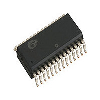
... GPIO pins can provide individual port over current inputs for each downstream USB port • Improved output drivers to reduce electromagnetic interference (EMI) • Operating voltage from 4.0V to 5.5V DC • Operating temperature from 0° to 70° C • Available in 28-pin SOIC (-SXC) package • Industry-standard programmer support. Document #: 38-08002 Rev. *D CY7C65113C Page ...
Page 6
... The microcontroller instruction set has been optimized specifically for USB operations, although the microcontrollers can be used for a variety of non-USB embedded applications. GPIO The CY7C65113C has 11 GPIO pins (P0[7:0], P1[2:0]), both rated per pin (typical) sink current. Multiple GPIO pins can be connected together to drive a single output for more drive current capacity. Clock The microcontroller uses an external 6-MHz crystal and an internal oscillator to provide a reference to an internal phase-locked loop (PLL)-based clock generator ...
Page 7
... P0[0] GPIO PORT 0 P0[7] P1[0] GPIO PORT 1 P1[ comp. SCLK SDATA Interface 2 *I C-compatible interface enabled by firmware through P1[1:0] CY7C65113C D+[0] Upstream USB Port D–[0] Downstream USB Ports USB D+[1] D–[1] Transceiver USB D+[2] Transceiver D–[2] USB D+[3] Transceiver D–[3] USB ...
Page 8
... GPIO Port 1 capable of sinking 7 mA (typical). 6-MHz crystal or external clock input. 6-MHz crystal out. Programming voltage supply, tie to ground during normal operation. Voltage supply. Ground. External 3.3V supply voltage for the downstream differential data output buffers and the D+ pull-up. CY7C65113C Page ...
Page 9
... USB Address A, Endpoint 3 in 5-endpoint mode 0x43 R/W USB Address B, Endpoint 1 Counter 0x44 R/W USB Address B, Endpoint 1 Configuration, or USB Address A, Endpoint 4 in 5-endpoint mode 0x48 R/W Hub Downstream Port Connect Status 0x49 R/W Hub Downstream Ports Enable 0x4A R/W Hub Downstream Ports Speed CY7C65113C Function Page ...
Page 10
... SWAP A,DSP 6 MOV [expr],A 7 MOV [X+expr], [expr], [X+expr],A 7 AND [expr],A 5 AND [X+expr],A 7 XOR [expr],A 8 XOR [X+expr],A 4 IOWX [X+expr] 5 CPL 6 ASL 4 ASR 5 RLC RRC CY7C65113C Function Page operand opcode cycles 20 4 acc direct 23 7 index 24 8 acc ...
Page 11
... Program Counter The 14-bit Program Counter (PC) allows access PROM available with the CY7C65113C architecture. The top 32 bytes of the ROM in the 8K part are reserved for testing purposes. The program counter is cleared during reset, such that the first instruction executed after a reset is at address 0x0000h. Typically, this is a jump instruction to a reset handler that initializes the application (see Interrupt Vectors on page 25) ...
Page 12
... USB address A endpoint 2 interrupt vector 0x000E USB address B endpoint 0 interrupt vector 0x0010 USB address B endpoint 1 interrupt vector 0x0012 Hub interrupt vector 0x0014 Reserved 0x0016 GPIO interrupt vector 2 0x0018 I C interrupt vector 0x001A Program Memory begins here 0x1FDF (8 KB -32) PROM ends here (CY7C65113C) CY7C65113C Page ...
Page 13
... Data Memory Organization The CY7C65113C microcontrollers provide 256 bytes of data RAM. Normally, the SRAM is partitioned into four areas: program stack, user variables, data stack, and USB endpoint FIFOs. The following is one example of where the program stack, data stack, and user variables areas could be located. ...
Page 14
... Move 20 hex into Accumulator (must be D8h or less) SWAP A,DSP ; swap accumulator value into DSP register. 5.6 Address Modes The CY7C65113 microcontrollers support three addressing modes for instructions that require data operands: data, direct, and indexed. 5.6.1 Data (Immediate) “Data” address mode refers to a data operand that is actually a constant encoded in the instruction example, consider the instruction that loads A with the constant 0xD8: • ...
Page 15
... Power-on Reset When V is first applied to the chip, the POR signal is asserted and the CY7C65113C enters a “semi-suspend” state. During CC the semi-suspend state, which is different from the suspend state defined in the USB specification, the oscillator and all other blocks of the part are functional, except for the CPU. This semi-suspend time ensures that both a valid V that the internal PLL has time to stabilize before full operation begins ...
Page 16
... Suspend Mode The CY7C65113C can be placed into a low-power state by setting the Suspend bit of the Processor Status and Control register. All logic blocks in the device are turned off except the GPIO interrupt logic and the USB receiver. The clock oscillator and PLL, as well as the free-running and Watchdog timers, are shut down ...
Page 17
... Figure 9-1. Block Diagram of a GPIO Pin P0.5 P0.4 P0.3 R/W R/W R Figure 9-2. Port 0 Data - - - - - - - - - - - - Figure 9-3. Port1 Data CY7C65113C Q2 GPIO PIN sink Address 0x00 2 1 P0.2 P0.1 P0.0 R/W R/W R Address 0x01 2 1 P1.2 P1.1 P1.0 R/W R/W R Page ...
Page 18
... During reset, all of the bits in the GPIO Configuration Register are written with ‘0’ to select Hi-Z mode for all GPIO ports as the default configuration. Document #: 38-08002 Rev Reserved Reserved Port 1 Config Bit R Figure 9-4. GPIO Configuration Register CY7C65113C Address 0x08 Port 1 Port 0 Port 0 Config Bit 0 Config Bit 1 Config Bit 0 R/W R/W R ...
Page 19
... P0.3 Intr Enable Enable Enable Figure 9-5. Port 0 Interrupt Enable Reserved Reserved Reserved - - - - - - Figure 9-6. Port 1 Interrupt Enable CY7C65113C Interrupt Polarity 0 Disabled 1 – (Falling Edge) 0 Disabled 1 Disabled 0 Disabled 1 – (Falling Edge) 0 Disabled 1 + (Rising Edge) Address 0x04 P0.2 Intr P0.1 Intr P0.0 Intr ...
Page 20
... Figure 10-2. Timer MSB Register Figure 10-3. Timer Block Diagram 2 The I C Position bit (Bit 7, Figure 11-1) and Reserved Reserved Reserved R/W R Figure 11- Configuration Register Port Width (Bit1, Figure 11-1) 0 CY7C65113C Address 0x24 Timer Bit 2 Timer Bit Address 0x25 Timer Bit 1.024-ms interrupt 128- µ ...
Page 21
... X 2 Figure 12- Data Register 2 C Bus Xmit Mode ACK R/W R Figure 12- Status and Control Register Description 2 C-compatible function is enabled. When cleared CY7C65113C 2 C Status and Control Register 2 C Status and Control 2 C-compatible functionality is 2 C-compatible block Data Data Data 1 R/W R/W ...
Page 22
... C Stop bit is generated restart sequence. The I 2 C-compatible function on the two I 2 C-compatible mode, the two pins operate in open drain mode, independent CY7C65113C 2 C Status and Control register. This 2 C start or restart target address for the restart must be written 2 C-compatible bus, 2 C-compatible pins ...
Page 23
... The Watchdog Reset does not effect the state of the POR and the Bus Reset Interrupt bits. Document #: 38-08002 Rev USB Bus Power-on Reset Reset Interrupt R/W R Figure 13-1. Processor Status and Control Register CY7C65113C Suspend Interrupt Reserved Enable Sense R ...
Page 24
... Interrupt Interrupt Enable Enable R Figure 14-1. Global Interrupt Enable Register 5 4 Reserved EPB1 EPB0 Interrupt Interrupt Enable Enable – R/W R/W – 0 CY7C65113C Address 0X20 1.024-ms 128-µs Interrupt Interrupt Enable Enable R/W R Address 0X21 EPA2 EPA1 Interrupt Interrupt Enable ...
Page 25
... Hub CLR Hub IRQ DAC CLR DAC IRQ GPIO CLR GPIO IRQ CLR IRQ Interrupt Priority Encoder Figure 14-3. Interrupt Controller Function Diagram CY7C65113C To CPU Vector CPU IRQ Sense IRQout Global Int Enable Interrupt Sense Enable Bit Controlled by DI, EI, and CLR ...
Page 26
... USB Address A Endpoint 1 interrupt 0x000C USB Address A Endpoint 2 interrupt 0x000E USB Address B Endpoint 0 interrupt 0x0010 USB Address B Endpoint 1 interrupt 0x0012 USB Hub interrupt 0x0014 DAC interrupt 0x0016 GPIO interrupt 2 0x0018 I C interrupt (10 clock cycles for the CALL instruction) + CY7C65113C Function Page ...
Page 27
... GPIO pin Global 1 = Enable GPIO Interrupt 0 = Disable Enable (Bit 5, Register 0x20) Figure 14-4. GPIO Interrupt Structure 2 C-compatible bus to signal the need for firmware interaction. This generally CY7C65113C GPIO Interrupt Flip Flop Interrupt Priority Encoder CLR 2 C registers. Refer IRQout Interrupt ...
Page 28
... After the hub is enumerated, the USB host can read hub connection status to determine which (if any) of the downstream ports need to be enumerated. The following is a brief summary of the typical enumeration process of the CY7C65113C by the USB host. For a detailed description of the enumeration process, refer to the USB specifi- cation. ...
Page 29
... These features are mapped onto a hub repeater and a hub controller. The hub controller is supported by the processor integrated into the CY7C65113C microcontroller. The hardware in the hub repeater detects whether a USB device is connected to a downstream port. The connection to a downstream port is through a differential signal pair (D+ and D–). Each downstream port provided by the hub requires external R device connected, the hub reads a LOW (zero) on both D+ and D– ...
Page 30
... Port 4 Speed Port 3 Speed Port 2 Speed Port 1 Speed R/W R/W R Figure 16-2. Hub Ports Speed Reserved Reserved Port 4 Enable Port 3 Enable Port 2 Enable Port 1 Enable R/W R/W R Figure 16-3. Hub Ports Enable Register CY7C65113C Address 0x4A R/W R/W R Address 0x49 R/W R/W R ...
Page 31
... Force Low D+[3] D–[3] D+[2] R/W R Figure 16-5. Hub Ports Force Low Register 5 4 Reserved Reserved Port 4 SE0 Status Figure 16-6. Hub Ports SE0 Status Register CY7C65113C Address 0x4B Port 2 Port 2 Port 1 Control Bit 0 Control Bit 1 R/W R/W R Force Low Force Low D– ...
Page 32
... Reserved Port 4 Diff. Data Figure 16-7. Hub Ports Data Register Reserved Reserved Port 4 Selective Suspend R/W R/W R Figure 16-8. Hub Ports Suspend Register CY7C65113C ADDRESS 0x50 Port 3 Diff. Port 2 Diff. Port 1 Diff. Data Data Data Address 0x4D Port 3 Port 2 Port 1 Selective ...
Page 33
... For normal USB operation, all of these bits must be cleared. Table 16-2 shows how the control bits affect the upstream port. Document #: 38-08002 Rev Reserved Reserved Resume Figure 16-9. Hub Ports Resume Status Register D– Bus Activity Upstream Upstream Figure 16-10. USB Status and Control Register CY7C65113C Address 0x4E Resume 3 Resume Address 0x1F Control Control Action Action Bit 2 Bit 1 R/W ...
Page 34
... The hub generates an EOP at EOF1 in accordance with the USB 1.1 Specification, Section 11.2.2 as well as USB 2.0 specification (section 11.2.5, page 304). 17.0 USB Serial Interface Engine Operation The CY7C65113C SIE supports operation as a single device or a compound device. This section describes the two device addresses, the configurable endpoints, and the endpoint function. 17.1 USB Device Addresses The USB Controller provides two USB Device Address Registers: A (addressed at 0x10)and B (addressed at 0x40) ...
Page 35
... EPA3 0xB8 8 EPA2 0xC0 32 EPA1 0xE0 32 EPA0 Endpoint 0 ACK IN OUT Received R/W R CY7C65113C [0,1] [1,1] One USB Address Endpoints) Start Address Size Label Start Address Size 0xD8 8 EPA3 0xE0 8 EPA4 0xE8 8 EPA0 0xF0 8 EPA1 0xF8 8 EPA2 Addresses 0x12(A0) and 0x42(B0 ...
Page 36
... Mode Bit 3 R/W R/W R Byte Count Byte Count Byte Count Bit 5 Bit 4 Bit 3 R/W R/W R Figure 17-4. USB Endpoint Counter Registers CY7C65113C [5] Addresses 0x14, 0x16, 0x44 Mode Bit 2 Mode Bit 1 R/W R Addresses 0x11, 0x13, 0x15, 0x41, 0x43 Byte Count Byte Count Bit 2 ...
Page 37
... For details on what conditions are required to generate an endpoint interrupt, refer to Table 18-2. 4. The contents of the updated endpoint 0 mode and counter registers are locked, except the SETUP bit of the endpoint 0 mode register which was locked earlier. Document #: 38-08002 Rev. *D CY7C65113C Page ...
Page 38
... Host To Device Data 1/0 Data Packet SETUP Host To Device Data 1/0 Data Packet Figure 17-5. Token/Data Packet Flow Diagram CY7C65113C Host To Device Hand Shake Packet UPDATE Device To Host C S ACK NAK STAL 16 C Hand Shake UPDATE Packet UPDATE only if FIFO is written Page ...
Page 39
... Is set by SIE on an ACK from mode 1101 (Ack In) TX Count ignore On issuance of an ACK this mode is changed by SIE to 1100 (NAK In) stall ignore NAK check Is set by SIE on an ACK from mode 1111 (Ack In – Status Out) – Status Out) CY7C65113C Comments Page ...
Page 40
... DTOG DVAL COUNT Setup Byte Count (bits 0..5, Figure 17-4) Data Valid (bit 6, Figure 17-4) Data0/1 (bit7 Figure 17-4) (Bit[7..5], Figure 17-2) The validity of the received data CY7C65113C In Out ACK Response SIE’s Response to the Host PID Status Bits Endpoint Mode bits ...
Page 41
... valid 1 1 updates UC valid 0 1 updates UC valid updates 1 updates invalid valid 1 1 updates UC valid 0 1 updates UC CY7C65113C In Out ACK Mode Bits Response ACK NoChange ignore NoChange ignore In Out ACK Mode Bits Response NoChange ignore NoChange NAK NoChange NAK NoChange ignore UC UC ...
Page 42
... updates updates updates updates Changes made by SIE to Internal Registers and Mode Bits dval DTOG DVAL COUNT Setup CY7C65113C Stall NoChange ignore NoChange ignore Stall In Out ACK Mode Bits Response ACK NoChange ignore NoChange ignore NoChange ignore [6] (STALL = NoChange Stall [6] (STALL = 1) UC ...
Page 43
... Endpoint 0 ACK Mode Bit 3 IN OUT Received Received Data Valid Byte Count Byte Count Byte Count Bit 5 Bit 4 Bit ACK Mode Bit 3 CY7C65113C Bit 2 Bit 1 Bit 0 Read/Write/B oth/–[7] P0.2 P0.1 P0.0 BBBBBBBB P1.2 P1.1 P1.0 BBBBBBBB P2.2 P2.1 P2.0 BBBBBBBB P3 ...
Page 44
... Diff. Data Force Low Force Low Force Low Force Low D–[4] D+[3] D–[3] D+[2] Watchdog USB Bus Power-on Suspend Reset Reset Reset Interrupt CY7C65113C Bit 2 Bit 1 Bit 0 Read/Write/B oth/–[7] Port 3 Port 2 Port 1 BBBBBBBB Connect Connect Connect Status Status Status Port 3 ...
Page 45
... D0– D1- D0+ D1+ D2- XTALO D2+ D3- XTALI D3+ GND GND D4- Vpp D4+ 15K(x8) (R UDN POWER MANAGEMENT .................................................................................................................... –0.5V to +7.0V CY7C65113C ) ext ) USB-A Vbus D– D+ GND USB-A Vbus D– D+ GND USB-A Vbus D– D+ GND USB-A Vbus D– D+ GND + 0. 0.5V ...
Page 46
... USB Upstream/Downstream Port 15 kΩ ±5% to Gnd 1.5 kΩ ± REF Including R Resistor ext General Purpose I/O (GPIO) All ports, low-to-high edge All ports, high-to-low edge 1.9 mA (all ports 0, below approximately 2.5V. CC CY7C65113C Min. Max. Unit 3.15 3.45 V –0.4 0 µ µA 1 0.2 V 0.8 2 ...
Page 47
... Per Table 7-6 of revision 1.1 of USB specification. CLOCK D+ D− Document #: 38-08002 Rev 6.0 MHz) OSC Description Clock Source [10] USB Full-speed Signaling / Timer Signals t CYC 90% 90% 10% CY7C65113C Min. Max. 6 ±0.25% 166.25 167.08 0.45 t CYC 0.45 t CYC 111 12 ±0.25% 8.192 14.336 t r 10% Page Unit MHz ...
Page 48
... SEATING PLANE 0.092[2.33] 0.105[2.67] 0.004[0.10] 0.004[0.10] * 0.0118[0.30 system, provided that the system conforms to the I CY7C65113C Operating Range Commercial Commercial MIN. MAX. PART # S28.3 STANDARD PKG. SZ28.3 LEAD FREE PKG. 0.0091[0.23] 0.015[0.38] 0.0125[3.17] 0.050[1.27] 51-85026-* Standard Specification ...
Page 49
... Document History Page Document Title: CY7C65113C USB Hub with Microcontroller Document Number: 38-08002 REV. ECN NO. Issue Date ** 109965 02/22/02 *A 120372 12/17/02 *B 124522 03/13/03 *C 368601 See ECN *D 429098 See ECN Document #: 38-08002 Rev. *D Orig. of Change SZV Change from Spec number: 38-00590 to 38-08002 MON Added register bit definitions ...