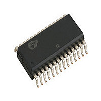
CY7C65113-SXC Cypress Semiconductor Corp, CY7C65113-SXC Datasheet - Page 14

CY7C65113-SXC
Manufacturer Part Number
CY7C65113-SXC
Description
Manufacturer
Cypress Semiconductor Corp
Datasheet
1.CY7C65113-SXC.pdf
(49 pages)
Specifications of CY7C65113-SXC
Operating Temperature (max)
70C
Operating Temperature (min)
0C
Operating Temperature Classification
Commercial
Package Type
SOIC
Mounting
Surface Mount
Lead Free Status / RoHS Status
Compliant
Available stocks
Company
Part Number
Manufacturer
Quantity
Price
Company:
Part Number:
CY7C65113-SXC
Manufacturer:
CYPRESS
Quantity:
770
Part Number:
CY7C65113-SXC
Manufacturer:
CYPRESS/赛普拉斯
Quantity:
20 000
Document #: 38-08002 Rev. *D
5.5
The Data Stack Pointer (DSP) supports PUSH and POP instructions that use the data stack for temporary storage. A PUSH
instruction pre-decrements the DSP, then writes data to the memory location addressed by the DSP. A POP instruction reads
data from the memory location addressed by the DSP, then post-increments the DSP.
During a reset, the DSP is reset to 0x00. A PUSH instruction when DSP equals 0x00 writes data at the top of the data RAM
(address 0xFF). This writes data to the memory area reserved for USB endpoint FIFOs. Therefore, the DSP should be indexed
at an appropriate memory location that does not compromise the Program Stack, user-defined memory (variables), or the USB
endpoint FIFOs.
For USB applications, the firmware should set the DSP to an appropriate location to avoid a memory conflict with RAM dedicated
to USB FIFOs. The memory requirements for the USB endpoints are described in Section 17.2. Example assembly instructions
to do this with two device addresses (FIFOs begin at 0xD8) are shown below:
5.6
The CY7C65113 microcontrollers support three addressing modes for instructions that require data operands: data, direct, and
indexed.
5.6.1
“Data” address mode refers to a data operand that is actually a constant encoded in the instruction. As an example, consider the
instruction that loads A with the constant 0xD8:
This instruction requires two bytes of code where the first byte identifies the “MOV A” instruction with a data operand as the
second byte. The second byte of the instruction is the constant “0xD8.” A constant may be referred to by name if a prior “EQU”
statement assigns the constant value to the name. For example, the following code is equivalent to the example shown above:
5.6.2
“Direct” address mode is used when the data operand is a variable stored in SRAM. In that case, the one byte address of the
variable is encoded in the instruction. As an example, consider an instruction that loads A with the contents of memory address
location 0x10:
Normally, variable names are assigned to variable addresses using “EQU” statements to improve the readability of the assembler
source code. As an example, the following code is equivalent to the example shown above:
5.6.3
“Indexed” address mode allows the firmware to manipulate arrays of data stored in SRAM. The address of the data operand is
the sum of a constant encoded in the instruction and the contents of the “X” register. Normally, the constant is the “base” address
of an array of data and the X register contains an index that indicates which element of the array is actually addressed:
This would have the effect of loading A with the fourth element of the SRAM “array” that begins at address 0x10. The fourth
element would be at address 0x13.
• MOV A, 0D8h.
• DSPINIT: EQU 0D8h
• MOV A, DSPINIT.
• MOV A, [10h].
• buttons: EQU 10h
• MOV A, [buttons].
• array: EQU 10h
• MOV X, 3
• MOV A, [X+array].
MOV A,20h
SWAP A,DSP ; swap accumulator value into DSP register.
8-bit Data Stack Pointer (DSP)
Address Modes
Data (Immediate)
Direct
Indexed
; Move 20 hex into Accumulator (must be D8h or less)
CY7C65113C
Page 14 of 49


