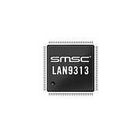
LAN9313I-NZW SMSC, LAN9313I-NZW Datasheet - Page 120

LAN9313I-NZW
Manufacturer Part Number
LAN9313I-NZW
Description
Ethernet ICs Three Port 10/100 Ethernet Switch
Manufacturer
SMSC
Type
Three Port Managed Ethernet Switchr
Datasheet
1.LAN9313-NZW.pdf
(399 pages)
Specifications of LAN9313I-NZW
Ethernet Connection Type
10 Base-T, 100 Base-TX
Minimum Operating Temperature
0 C
Mounting Style
SMD/SMT
Product
Ethernet Switches
Number Of Transceivers
1
Standard Supported
802.3, 802.3u
Data Rate
10 Mbps, 100 Mbps
Supply Voltage (max)
3.3 V
Supply Voltage (min)
0 V
Supply Current (max)
155 mA, 270 mA
Maximum Operating Temperature
+ 70 C
Package / Case
TQFP-100
Lead Free Status / RoHS Status
Lead free / RoHS Compliant
Available stocks
Company
Part Number
Manufacturer
Quantity
Price
Company:
Part Number:
LAN9313I-NZW
Manufacturer:
Standard
Quantity:
261
Company:
Part Number:
LAN9313I-NZW
Manufacturer:
Microchip Technology
Quantity:
10 000
- Current page: 120 of 399
- Download datasheet (5Mb)
Revision 1.7 (06-29-10)
8.4.1.1
8.4.2
SCK (active high)
SCK (active low)
nSCS
SO
SCK (active high)
SI
SCK (active low)
Figure 8.1
SPI Read Polling for Reset Complete
During reset, the SPI slave interface will not return valid data. To determine when the reset condition
is complete, the
read, the interface can be considered functional. At this point, the READY bit in the
Configuration Register (HW_CFG)
complete. Refer to
SPI Write Sequence
The SPI slave interface of the LAN9313/LAN9313i is selected for writes by first bringing nSCS low.
The SI pin should then driven with an 8-bit write instruction, followed by the 8-bit address and then the
data.
Multiple writes are performed by continuing the clock pulses and input data while nSCS is low.
Depending on the instruction (as shown in
decremented, or maintained. Maintaining an fixed internal address is useful for “bit-banging”. For auto-
incrementing instructions, once the internal address reaches its maximum, it rolls over to 0. For auto-
decrementing instructions, once the internal address reaches 0, it rolls over to its maximum.
The nSCS input is brought high to conclude the cycle. The SO output is three-stated throughout the
entire write sequence.
The data write to the register occurs after the 32-bits are input. In the event that 32-bits are not written
when the nSCS is returned high, the write is considered invalid and the register is not affected. Multiple
registers may be written in a multiple write cycle, each one being written after 32-bits.
SPI writes must not be performed to unused register addresses.
X
X
X
1
0
1
nSCS
2
0
SO
2
SI
3
0
illustrates a typical single and multiple register read.
3
X
X
Instruction
X
4
0
4
1
5
0
dec
1
Byte Order Test Register (BYTE_TEST)
5
2
0
6
2
Section 4.2, "Resets," on page 41
inc
6
3
0
7
3
1
7
Instruction
4
0
8
4
1
8
Z
5
9
0
5
A9
9
6
0
1
0
6
A8
Figure 8.1 SPI Reads
1
0
7
1
1
1
7
A7
DATASHEET
1
1
8
Multiple Register Reads
Single Register Read
1
2
1
Address
can be polled to determine when the device initialization is
Z
8
A6
1
2
9
A9
1
3
9
A5
1
3
120
1
0
A8
1
4
1
0
A4
1
4
1
1
A7
1
5
1
1
A3
1
5
Table
1
2
Address
A6
1
6
1
2
A2
1
6
1
3
A5
1
7
1
3
31
D
1
7
for additional information.
1
4
8.10), the internal address is incremented,
Data 1...
A4
1
8
1
4
30
X
D
1
8
should be polled. Once the correct pattern is
1
5
A3
1
9
1
5
29
.. .
D
1
9
1
6
.. .
A2
.. .
.. .
Three Port 10/100 Managed Ethernet Switch with MII
1
6
1
7
31
D
…Data m
1
7
1
8
D2
30
X
D
1
8
1
9
D1
29
.. .
D
1
9
.. .
.. .
.. .
D0
Data
4
5
X
4
5
31
D
Data m+1...
4
6
SMSC LAN9313/LAN9313i
D2
4
6
30
D
4
7
D1
4
7
29
.. .
D
X
4
8
.. .
D0
.. .
.. .
4
8
X
X
…Data n
X
Z
D2
Hardware
Datasheet
D1
X
D0
X
X
X
Z
Related parts for LAN9313I-NZW
Image
Part Number
Description
Manufacturer
Datasheet
Request
R

Part Number:
Description:
Three Port 10/100 Managed Ethernet Switch with MII
Manufacturer:
SMSC [SMSC Corporation]
Datasheet:

Part Number:
Description:
Ethernet ICs Three Port 10/100 Ethernet Switch
Manufacturer:
SMSC
Datasheet:

Part Number:
Description:
Ethernet ICs Three Port 10/100 Ethernet Switch
Manufacturer:
SMSC
Datasheet:

Part Number:
Description:
FAST ETHERNET PHYSICAL LAYER DEVICE
Manufacturer:
SMSC Corporation
Datasheet:

Part Number:
Description:
357-036-542-201 CARDEDGE 36POS DL .156 BLK LOPRO
Manufacturer:
SMSC Corporation
Datasheet:

Part Number:
Description:
357-036-542-201 CARDEDGE 36POS DL .156 BLK LOPRO
Manufacturer:
SMSC Corporation
Datasheet:

Part Number:
Description:
357-036-542-201 CARDEDGE 36POS DL .156 BLK LOPRO
Manufacturer:
SMSC Corporation
Datasheet:

Part Number:
Description:
4-PORT USB2.0 HUB CONTROLLER
Manufacturer:
SMSC Corporation
Datasheet:

Part Number:
Description:
Manufacturer:
SMSC Corporation
Datasheet:

Part Number:
Description:
Manufacturer:
SMSC Corporation
Datasheet:

Part Number:
Description:
FDC37C672ENHANCED SUPER I/O CONTROLLER WITH FAST IR
Manufacturer:
SMSC Corporation
Datasheet:

Part Number:
Description:
COM90C66LJPARCNET Controller/Transceiver with AT Interface and On-Chip RAM
Manufacturer:
SMSC Corporation
Datasheet:

Part Number:
Description:
Manufacturer:
SMSC Corporation
Datasheet:

Part Number:
Description:
Manufacturer:
SMSC Corporation
Datasheet:


