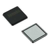
JN5148-001-X NXP Semiconductors, JN5148-001-X Datasheet - Page 63

JN5148-001-X
Manufacturer Part Number
JN5148-001-X
Description
IC MCU 802.15.4 32BIT 2.4G 56QFN
Manufacturer
NXP Semiconductors
Series
JN5148r
Datasheet
1.JN5148-UG010.pdf
(99 pages)
Specifications of JN5148-001-X
Frequency
2.4GHz
Data Rate - Maximum
667kbps
Modulation Or Protocol
802.15.4
Applications
Home/Building Automation, Industrial Control
Power - Output
2.5dBm
Sensitivity
-95dBm
Voltage - Supply
2 V ~ 3.6 V
Current - Receiving
17.5mA
Current - Transmitting
15mA
Data Interface
PCB, Surface Mount
Memory Size
128kB RAM, 128kB ROM
Antenna Connector
PCB, Surface Mount
Operating Temperature
-40°C ~ 85°C
Package / Case
56-QFN
Lead Free Status / RoHS Status
Lead free / RoHS Compliant
Other names
616-1049-2
935293999531
JN5148-001-X
935293999531
JN5148-001-X
and this therefore preserves any interface to the outside world. The DAC outputs are placed into a high impedance
state.
When entering into sleep mode, there is an option to retain the RAM contents throughout the sleep period. If the
wakeup timers are not to be used for a wakeup event and the application does not require them to run continually,
then power can be saved by switching off the 32kHz oscillator if selected as the system clock through software
control. The oscillator will be restarted when a wakeup event occurs.
Whilst in sleep mode one of four possible events can cause a wakeup to occur: transitions on DIO inputs, expiry of
wakeup timers, pulse counters maturing or comparator events. If any of these events occur, and the relevant
interrupt is enabled, then an interrupt is generated that will cause a wakeup from sleep. It is possible for multiple
wakeup sources to trigger an event at the same instant and only one of them will be accountable for the wakeup
period. It is therefore necessary in software to remove all other pending wakeup events prior to requesting entry back
into sleep mode; otherwise, the device will re-awaken immediately.
When wakeup occurs, a similar sequence of events to the reset process described in section 6.1 happens, including
the checking of the supply voltage by the Brown Out Detector 6.4. The 32MHz oscillator is started up, once stable
the power to CPU system is enabled and the reset is removed. Software determines that this is a reset from sleep
and so commences with the wakeup process. If RAM contents were held through sleep, wakeup is quicker as the
application program does not have to be reloaded from Flash memory. See section 22.3.6 for wake-up timings.
21.3.1 Wakeup Timer Event
The JN5148 contains two 35-bit wakeup timers that are counters clocked from the 32kHz oscillator, and can be
programmed to generate a wake-up event. Following a wakeup event, the timers continue to run. These timers are
described in section 11.3.
Timer events can be generated from both of the two timers; one is intended for use by the 802.15.4 protocol, the
other being available for use by the Application running on the CPU. These timers are available to run at any time,
even during sleep mode.
21.3.2 DIO Event
Any DIO pin when used as an input has the capability, by detecting a transition, to generate a wake-up event. Once
this feature has been enabled the type of transition can be specified (rising or falling edge). Even when groups of
DIO lines are configured as alternative functions such as the UARTs or Timers etc, any input line in the group can still
be used to provide a wakeup event. This means that an external device communicating over the UART can wakeup
a sleeping device by asserting its RTS signal pin (which is the CTS input of the JN5148).
21.3.3 Comparator Event
The comparator can generate a wakeup interrupt when a change in the relative levels of the positive and negative
inputs occurs. The ability to wakeup when continuously monitoring analogue signals is useful in ultra-low power
applications. For example, the JN5148 can remain in sleep mode until the voltage drops below a threshold and then
be woken up to deal with the alarm condition.
21.3.4 Pulse Counter
The JN5148 contains two 16 bit pulse counters that can be programmed to generate a wake-up event. Following the
wakeup event the counters will continue to operate and therefore no pulse will be missed during the wake-up
process. These counters are described in section 12.
To minimise sleep current it is possible to disable the 32K RC oscillator and still use the pulse counters to cause a
wake-up event, provided debounce mode is not required.
21.4 Deep Sleep Mode
Deep sleep mode gives the lowest power consumption. All switchable power domains are off and certain functions in
the VDD supply power domain, including the 32kHz oscillator are stopped. This mode can be exited by a power
down, a hardware reset on the RESETN pin, or a DIO event. The DIO event in this mode causes a chip reset to
occur.
© NXP Laboratories UK 2010
JN-DS-JN5148-001 1v6
63


