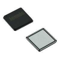
JN5148-001-X NXP Semiconductors, JN5148-001-X Datasheet - Page 13

JN5148-001-X
Manufacturer Part Number
JN5148-001-X
Description
IC MCU 802.15.4 32BIT 2.4G 56QFN
Manufacturer
NXP Semiconductors
Series
JN5148r
Datasheet
1.JN5148-UG010.pdf
(99 pages)
Specifications of JN5148-001-X
Frequency
2.4GHz
Data Rate - Maximum
667kbps
Modulation Or Protocol
802.15.4
Applications
Home/Building Automation, Industrial Control
Power - Output
2.5dBm
Sensitivity
-95dBm
Voltage - Supply
2 V ~ 3.6 V
Current - Receiving
17.5mA
Current - Transmitting
15mA
Data Interface
PCB, Surface Mount
Memory Size
128kB RAM, 128kB ROM
Antenna Connector
PCB, Surface Mount
Operating Temperature
-40°C ~ 85°C
Package / Case
56-QFN
Lead Free Status / RoHS Status
Lead free / RoHS Compliant
Other names
616-1049-2
935293999531
JN5148-001-X
935293999531
JN5148-001-X
2.2.5 Analogue Peripherals
Several of the analogue peripherals require a reference voltage to use as part of their operations. They can use
either an internal reference voltage or an external reference connected to VREF. This voltage is referenced to
analogue ground and the performance of the analogue peripherals is dependant on the quality of this reference.
There are four ADC inputs, two pairs of comparator inputs and two DAC outputs. The analogue I/O pins on the
JN5148 can have signals applied up to 0.3v higher than VDD1. A schematic view of the analogue I/O cell is shown in
Figure 3: Analogue I/O Cell
In reset and deep sleep, the analogue peripherals are all off and the DAC outputs are in a high impedance state.
In sleep, the ADC and DACs are off, with the DAC outputs in high impedance state. The comparators may optionally
be used as a wakeup source.
Unused ADC and comparator inputs should be left unconnected.
VDD1
Analogue
I/O Pin
Analogue
Peripheral
VSSA
Figure 3: Analogue I/O Cell
2.2.6 Digital Input/Output
Digital I/O pins on the JN5148 can have signals applied up to 2V higher than VDD2 (with the exception of pins DIO9
and DIO10 that are 3V tolerant) and are therefore TTL-compatible with VDD2 > 3V. For other DC properties of these
pins see section 22.2.3 I/O Characteristics.
When used in their primary function all Digital Input/Output pins are bi-directional and are connected to weak internal
pull up resistors (40kΩ nominal) that can be disabled. When used in their secondary function (selected when the
appropriate peripheral block is enabled through software library calls) then their direction is fixed by the function. The
pull up resistor is enabled or disabled independently of the function and direction; the default state from reset is
enabled.
A schematic view of the digital I/O cell is in Figure 4: DIO Pin Equivalent Schematic.
© NXP Laboratories UK 2010
JN-DS-JN5148-001 1v6
13


