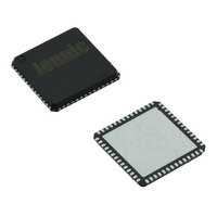
JN5148-001-X NXP Semiconductors, JN5148-001-X Datasheet - Page 41

JN5148-001-X
Manufacturer Part Number
JN5148-001-X
Description
IC MCU 802.15.4 32BIT 2.4G 56QFN
Manufacturer
NXP Semiconductors
Series
JN5148r
Datasheet
1.JN5148-UG010.pdf
(99 pages)
Specifications of JN5148-001-X
Frequency
2.4GHz
Data Rate - Maximum
667kbps
Modulation Or Protocol
802.15.4
Applications
Home/Building Automation, Industrial Control
Power - Output
2.5dBm
Sensitivity
-95dBm
Voltage - Supply
2 V ~ 3.6 V
Current - Receiving
17.5mA
Current - Transmitting
15mA
Data Interface
PCB, Surface Mount
Memory Size
128kB RAM, 128kB ROM
Antenna Connector
PCB, Surface Mount
Operating Temperature
-40°C ~ 85°C
Package / Case
56-QFN
Lead Free Status / RoHS Status
Lead free / RoHS Compliant
Other names
616-1049-2
935293999531
JN5148-001-X
935293999531
JN5148-001-X
- Current page: 41 of 99
- Download datasheet (649Kb)
11.1.5 Example Timer / Counter Application
Figure 31 shows an application of the JN5148 timers to provide closed loop speed control. Timer 0 is configured in
PWM mode to provide a variable mark-space ratio switching waveform to the gate of the NFET. This in turn controls
the power in the DC motor.
Timer 1 is configured to count the rising edge events on the clk/gate pin over a constant period. This converts the
tacho pulse stream output into a count proportional to the motor speed. This value is then used by the application
software executing the control algorithm.
If required for other functionality, then the unused IO associated with the timers could be used as general purpose
DIO.
11.2 Tick Timer
The JN5148 contains a hardware timer that can be used for generating timing interrupts to software. It may be used
to implement regular events such as ticks for software timers or an operating system, as a high-precision timing
reference or can be used to implement system monitor timeouts as used in a watchdog timer. Features include:
© NXP Laboratories UK 2010
•
32-bit counter
1
Timer 0
Timer 1
2
JN5148
Figure 31: Closed Loop PWM Speed Control Using JN5148 Timers
51
48
50
52
53
54
Conversion cycle 1
CLK/GATE
CAPTURE
CLK/GATE
CAPTURE
PWM
PWM
3
Figure 29: Return To Zero Mode in Operation
1
2
Figure 30: Non-Return to Zero Mode
Conversion cycle 1
3
JN-DS-JN5148-001 1v6
N
1N4007
N
2
16
2
17
1
Conversion cycle 2
2
1
M
IRF521
3
2
1 pulse/rev
Conversion cycle 2
N
3
Tacho
+12V
N
41
Related parts for JN5148-001-X
Image
Part Number
Description
Manufacturer
Datasheet
Request
R

Part Number:
Description:
The JN5148 is an ultra low power, high performance MCU combined with an IEEE802
Manufacturer:
NXP Semiconductors
Datasheet:

Part Number:
Description:
Microcontrollers (MCU) 32bit RISC 32MHz
Manufacturer:
NXP Semiconductors
Datasheet:

Part Number:
Description:
Microcontrollers (MCU) 32bit RISC 32MHz
Manufacturer:
NXP Semiconductors

Part Number:
Description:
Zigbee / 802.15.4 Modules & Development Tools Lo-Power RF Solution Jennic Demo Board
Manufacturer:
NXP Semiconductors
Datasheet:

Part Number:
Description:
Microcontrollers (MCU) 32bit RISC 2.4GHz
Manufacturer:
NXP Semiconductors
Datasheet:

Part Number:
Description:
MODULE ZIGBEE PRO U.FL CONN
Manufacturer:
NXP Semiconductors
Datasheet:

Part Number:
Description:
MODULE ZIGBEE PRO CERM ANTENNA
Manufacturer:
NXP Semiconductors
Datasheet:

Part Number:
Description:
MODULE ZIGBEE PRO HP U.FL CONN
Manufacturer:
NXP Semiconductors
Datasheet:
Part Number:
Description:
MCU 802.15.4 32BIT 2.4G 56-QFN
Manufacturer:
NXP Semiconductors
Datasheet:
Part Number:
Description:
MCU 802.15.4 32BIT 2.4G 56-QFN
Manufacturer:
NXP Semiconductors
Datasheet:

Part Number:
Description:
Microcontrollers (MCU) 32bit RISC 32MHz
Manufacturer:
NXP Semiconductors
Part Number:
Description:
NXP Semiconductors designed the LPC2420/2460 microcontroller around a 16-bit/32-bitARM7TDMI-S CPU core with real-time debug interfaces that include both JTAG andembedded trace
Manufacturer:
NXP Semiconductors
Datasheet:

Part Number:
Description:
NXP Semiconductors designed the LPC2458 microcontroller around a 16-bit/32-bitARM7TDMI-S CPU core with real-time debug interfaces that include both JTAG andembedded trace
Manufacturer:
NXP Semiconductors
Datasheet:
Part Number:
Description:
NXP Semiconductors designed the LPC2468 microcontroller around a 16-bit/32-bitARM7TDMI-S CPU core with real-time debug interfaces that include both JTAG andembedded trace
Manufacturer:
NXP Semiconductors
Datasheet:
Part Number:
Description:
NXP Semiconductors designed the LPC2470 microcontroller, powered by theARM7TDMI-S core, to be a highly integrated microcontroller for a wide range ofapplications that require advanced communications and high quality graphic displays
Manufacturer:
NXP Semiconductors
Datasheet:


