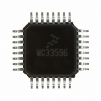
MC33596FJE Freescale Semiconductor, MC33596FJE Datasheet - Page 55

MC33596FJE
Manufacturer Part Number
MC33596FJE
Description
IC RECEIVER UHF PLL TUNED 32LQFP
Manufacturer
Freescale Semiconductor
Type
Receiverr
Datasheet
1.MC33596FCAE.pdf
(70 pages)
Specifications of MC33596FJE
Frequency
304, 315, 426, 434, 868 & 915MHz
Sensitivity
-104dBm
Data Rate - Maximum
22.4 kBaud
Modulation Or Protocol
FSK, OOK
Applications
General Data Transfer
Current - Receiving
10.3mA
Data Interface
PCB, Surface Mount
Antenna Connector
PCB, Surface Mount
Voltage - Supply
2.7 V ~ 3.6 V, 4.5 V ~ 5.5 V
Operating Temperature
-40°C ~ 85°C
Package / Case
32-LQFP
Operating Frequency
915 MHz
Operating Supply Voltage
3.3 V or 5 V
Maximum Operating Temperature
+ 85 C
Minimum Operating Temperature
- 40 C
Mounting Style
SMD/SMT
Operating Temperature (min)
-40C
Operating Temperature (max)
85C
Operating Temperature Classification
Industrial
Modulation Type
FSK/OOK
Package Type
LQFP
Operating Supply Voltage (min)
2.7V
Lead Free Status / RoHS Status
Lead free / RoHS Compliant
Features
-
Memory Size
-
Lead Free Status / Rohs Status
Lead free / RoHS Compliant
Available stocks
Company
Part Number
Manufacturer
Quantity
Price
Part Number:
MC33596FJE
Manufacturer:
FREESCALE
Quantity:
20 000
Part Number:
MC33596FJER2
Manufacturer:
FREESCALE
Quantity:
20 000
19.6 Digital Input: CONFB, MOSI, SCLK, SEB, STROBE,
NOTES:
1
2
19.7 Digital Output
Freescale Semiconductor
Operating supply voltage and temperature range see
schematic (see
3.0 V, T
Operating supply voltage and temperature range see
schematic (see
3.0 V, T
7.10 Input low voltage
7.11 Input high voltage
7.12 Input hysteresis
7.7 Input low voltage
7.8 Input high voltage
7.9 Input hysteresis
7.5 Sink current
7.6
8.1 Output low voltage
8.2 Output high voltage
8.3 Fall and rise time
8.4 Output low voltage
8.5 Output high voltage
Input levels of those pins are referenced to V
Input levels of those pins are referenced to V
A
A
= 25°C.
= 25°C.
RSSIC
Figure 43
Figure 43
Parameter
Parameter
through
through
Figure
Figure
Digital Output: DATACLK, LVD, MISO, MOSI, SCLK
MOSI, SCLK, SEB, RSSIC
CONFB, STROBE
Configuration, receive, modes
standby or LVD modes
54), unless otherwise specified. Typical values reflect average measurement at V
54), unless otherwise specified. Typical values reflect average measurement at V
|
From 10% to 90% of the
output swing,
C
|
ILOAD|
ILOAD|
LOAD
CC2
CCDIG2
Digital Output: SWITCH (V
Test Conditions
MC33596 Data Sheet, Rev. 4
Test Conditions
= 50 μA
= 10pF
= 50 μA
Comments
which depends upon V
Comments
Table
Table
which depends upon the circuit state (see
2
3. Values refer to the circuit recommended in the application
3. Values refer to the circuit recommended in the application
(1)
0.8 x V
0.1 x V
CC
0.8 x V
0.8 x V
0.1 x V
0.8 x V
CC
(see
Min
Min
0.5
= 3V)
—
—
—
—
—
1
CCDIG2
CCDIG2
CCIO
CC2
CC2
Section 5, “Power
CC
Limits
Limits
Typ
Typ
80
—
—
—
—
—
—
—
—
—
—
—
—
Section 5, “Power
Electrical Characteristics
Supply”).
0.4 x V
0.2 x V
0.4 x V
0.2 x V
Max
Max
100
150
10
—
—
—
—
—
—
CCDIG2
CCIO
CC2
CC
Supply”).
Unit
Unit
nA
nA
ns
V
V
V
V
V
V
V
V
V
V
CC
CC
55
=
=


