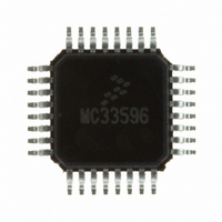
MC33596FJE Freescale Semiconductor, MC33596FJE Datasheet - Page 38

MC33596FJE
Manufacturer Part Number
MC33596FJE
Description
IC RECEIVER UHF PLL TUNED 32LQFP
Manufacturer
Freescale Semiconductor
Type
Receiverr
Datasheet
1.MC33596FCAE.pdf
(70 pages)
Specifications of MC33596FJE
Frequency
304, 315, 426, 434, 868 & 915MHz
Sensitivity
-104dBm
Data Rate - Maximum
22.4 kBaud
Modulation Or Protocol
FSK, OOK
Applications
General Data Transfer
Current - Receiving
10.3mA
Data Interface
PCB, Surface Mount
Antenna Connector
PCB, Surface Mount
Voltage - Supply
2.7 V ~ 3.6 V, 4.5 V ~ 5.5 V
Operating Temperature
-40°C ~ 85°C
Package / Case
32-LQFP
Operating Frequency
915 MHz
Operating Supply Voltage
3.3 V or 5 V
Maximum Operating Temperature
+ 85 C
Minimum Operating Temperature
- 40 C
Mounting Style
SMD/SMT
Operating Temperature (min)
-40C
Operating Temperature (max)
85C
Operating Temperature Classification
Industrial
Modulation Type
FSK/OOK
Package Type
LQFP
Operating Supply Voltage (min)
2.7V
Lead Free Status / RoHS Status
Lead free / RoHS Compliant
Features
-
Memory Size
-
Lead Free Status / Rohs Status
Lead free / RoHS Compliant
Available stocks
Company
Part Number
Manufacturer
Quantity
Price
Part Number:
MC33596FJE
Manufacturer:
FREESCALE
Quantity:
20 000
Part Number:
MC33596FJER2
Manufacturer:
FREESCALE
Quantity:
20 000
Register Description
AFFC (Average Filter Frequency Control) enables direct control of the average filter cut-off frequency.
IFLA (IF Level Attenuation) controls the maximum gain of the IF amplifier in OOK modulation.
The reduction in gain can be observed if the IF amplifier AGC system is disabled (by setting RAGC = 1).
RSSIE (RSSI Enable) enables the RSSI function.
EDD (Envelop Detector Decay) controls the envelop detector decay.
RAGC (Reset Automatic Gain Control) resets both receiver internal AGCs.
A first SPI access allows RAGC to be set; a second SPI access is required to reset it.
FAGC (Freeze Automatic Gain Control) freezes both receiver AGC levels.
BANKS indicates which register bank is active. This bit, available in Bank A and Bank B, returns the same
value.
16.3 Frequency Register
Figure 28
38
Reset Value
Bit Name
Access
0 = Average filter cut-off frequency is defined by DR[1:0]
1 = Average filter cut-off frequency is defined by AFF[1:0]
0 = No effect
1 = Decreases by 20 dB (typical) the maximum gain of the IF amplifier, in OOK modulation only
0 = Disabled
1 = Enabled
0 = Slow decay for minimum ripple
1 = Fast decay
0 = No action
1 = Sets the gain to its maximum value
0 = No action
1= Holds the gain at its current value
0 = Bank B
1 = Bank A
defines the Frequency register, F.
AFFC
Bit 7
R/W
0
IFLA
Bit 6
R/W
0
Figure 27. COMMAND Register
Bit 5
—
—
0
MC33596 Data Sheet, Rev. 4
RSSIE
Bit 4
R/W
0
Bit 3
EDD
R/W
1
RAGC
Bit 2
R/W
0
FAGC
Bit 1
R/W
0
Freescale Semiconductor
BANKS
Bit 0
R
1
Addr
$03


