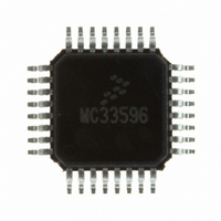
MC33596FJE Freescale Semiconductor, MC33596FJE Datasheet - Page 12

MC33596FJE
Manufacturer Part Number
MC33596FJE
Description
IC RECEIVER UHF PLL TUNED 32LQFP
Manufacturer
Freescale Semiconductor
Type
Receiverr
Datasheet
1.MC33596FCAE.pdf
(70 pages)
Specifications of MC33596FJE
Frequency
304, 315, 426, 434, 868 & 915MHz
Sensitivity
-104dBm
Data Rate - Maximum
22.4 kBaud
Modulation Or Protocol
FSK, OOK
Applications
General Data Transfer
Current - Receiving
10.3mA
Data Interface
PCB, Surface Mount
Antenna Connector
PCB, Surface Mount
Voltage - Supply
2.7 V ~ 3.6 V, 4.5 V ~ 5.5 V
Operating Temperature
-40°C ~ 85°C
Package / Case
32-LQFP
Operating Frequency
915 MHz
Operating Supply Voltage
3.3 V or 5 V
Maximum Operating Temperature
+ 85 C
Minimum Operating Temperature
- 40 C
Mounting Style
SMD/SMT
Operating Temperature (min)
-40C
Operating Temperature (max)
85C
Operating Temperature Classification
Industrial
Modulation Type
FSK/OOK
Package Type
LQFP
Operating Supply Voltage (min)
2.7V
Lead Free Status / RoHS Status
Lead free / RoHS Compliant
Features
-
Memory Size
-
Lead Free Status / Rohs Status
Lead free / RoHS Compliant
Available stocks
Company
Part Number
Manufacturer
Quantity
Price
Part Number:
MC33596FJE
Manufacturer:
FREESCALE
Quantity:
20 000
Part Number:
MC33596FJER2
Manufacturer:
FREESCALE
Quantity:
20 000
Receive Mode
11
The receiver is either waiting for an RF transmission or is receiving one. Two different processes are
possible, as determined by the values of the DME bit. A state diagram describes the sequence of operations
in each case.
11.1 Data Manager Disabled (DME=0)
Data manager disabled means that the SPI is deselected and raw data is sent directly on the MOSI line,
while SCLK remains at low level.
Two different processes are possible, as determined by the values of the SOE bit.
11.1.1 Data Manager Disabled and Strobe Pin Control
Raw received data is sent directly on the MOSI line.
For all states: At any time, a low level applied to CONFB forces the state machine to state 1, configuration
mode.
12
•
•
State 5:
The receiver is in standby/LVD mode. For further information, see
Mode.” A high level applied to STROBE forces the circuit to state 5b.
State 5b:
The receiver is kept on by the STROBE pin. Raw data is output on the MOSI line.
Receive Mode
If the STROBE pin is tied to a high level before switching to receive mode,
the receiver does not go through an off or standby state.
STROBE = 1
Figure 3. Receive Mode, DME = 0, SOE = 0
MC33596 Data Sheet, Rev. 4
Raw Data on MOSI
Standby/LVD
State 5b
State 5
NOTE
On
STROBE = 0
STROBE = 1
Figure 3
shows the state diagram.
STROBE = 0
Section 12, “Standby: LVD
SPI Deselected
Freescale Semiconductor


