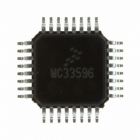
MC33596FJE Freescale Semiconductor, MC33596FJE Datasheet - Page 10

MC33596FJE
Manufacturer Part Number
MC33596FJE
Description
IC RECEIVER UHF PLL TUNED 32LQFP
Manufacturer
Freescale Semiconductor
Type
Receiverr
Datasheet
1.MC33596FCAE.pdf
(70 pages)
Specifications of MC33596FJE
Frequency
304, 315, 426, 434, 868 & 915MHz
Sensitivity
-104dBm
Data Rate - Maximum
22.4 kBaud
Modulation Or Protocol
FSK, OOK
Applications
General Data Transfer
Current - Receiving
10.3mA
Data Interface
PCB, Surface Mount
Antenna Connector
PCB, Surface Mount
Voltage - Supply
2.7 V ~ 3.6 V, 4.5 V ~ 5.5 V
Operating Temperature
-40°C ~ 85°C
Package / Case
32-LQFP
Operating Frequency
915 MHz
Operating Supply Voltage
3.3 V or 5 V
Maximum Operating Temperature
+ 85 C
Minimum Operating Temperature
- 40 C
Mounting Style
SMD/SMT
Operating Temperature (min)
-40C
Operating Temperature (max)
85C
Operating Temperature Classification
Industrial
Modulation Type
FSK/OOK
Package Type
LQFP
Operating Supply Voltage (min)
2.7V
Lead Free Status / RoHS Status
Lead free / RoHS Compliant
Features
-
Memory Size
-
Lead Free Status / Rohs Status
Lead free / RoHS Compliant
Available stocks
Company
Part Number
Manufacturer
Quantity
Price
Part Number:
MC33596FJE
Manufacturer:
FREESCALE
Quantity:
20 000
Part Number:
MC33596FJER2
Manufacturer:
FREESCALE
Quantity:
20 000
State Machine
Refer to
be complied with in order to change between two selected modes.
The data transfer protocol for each mode is described in the following section.
10
This section describes how the MC33596 controller executes sequences of operations, relative to the
selected mode. The controller is a finite state machine, clocked at T
Figure 2
There are three different modes: configuration, receive, and standby/LVD. Each mode is exclusive and can
be entered in different ways, as follows.
After a Power-on Reset (POR), the circuit is in standby mode (see
contents are set to the reset value.
At any time, a low level applied to CONFB forces the finite state machine into configuration mode,
whatever the current state. This is not always shown in state diagrams, but must always be considered.
Refer to
and configuration mode.
10
•
•
•
External signal: CONFB for configuration mode
External signal and configuration bits: CONFB and TRXE for all other modes,
External signal and internal conditions: see
enter standby/LVD mode
Configuration
Receive
Standby / LVD
(Section 14, “Power-On Reset and MC33596
Section 10, “State
(note that some branches refer to other diagrams that provide more detailed information).
State Machine
Selected Mode
DME = 1
DME = 0
Table 5. Serial Digital Interface Feature versus Selected Mode
Machine,” and to
SPI slave, data received on MOSI, SCLK from MCU, MISO is output (SEB=0)
SPI master, data sent on MOSI with clock on SCLK (SEB=0)
SPI deselected, received data are directly sent to MOSI (SEB=0)
SPI deselected, all I/O are high impedance (SEB =1)
MC33596 Data Sheet, Rev. 4
Figure 2
MC33596 Digital Interface Use
Figure 3
Startup”) for timing sequence between standy mode
for more details about all the conditions that must
and
Figure 12
Figure
digclk
. An overview is presented in
2) and the configuration register
for information on how to
Freescale Semiconductor


