MC56F8037VLH Freescale Semiconductor, MC56F8037VLH Datasheet - Page 31
MC56F8037VLH
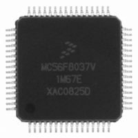
Manufacturer Part Number
MC56F8037VLH
Description
IC DSP 16BIT DUAL 64-LQFP
Manufacturer
Freescale Semiconductor
Series
56F8xxxr
Datasheet
1.MC56F8037EVM.pdf
(180 pages)
Specifications of MC56F8037VLH
Core Processor
56800
Core Size
16-Bit
Speed
32MHz
Connectivity
CAN, I²C, SCI, SPI
Peripherals
POR, PWM, WDT
Number Of I /o
53
Program Memory Size
64KB (32K x 16)
Program Memory Type
FLASH
Ram Size
4K x 16
Voltage - Supply (vcc/vdd)
3 V ~ 3.6 V
Data Converters
A/D 16x12b; D/A 2x12b
Oscillator Type
Internal
Operating Temperature
-40°C ~ 105°C
Package / Case
64-LQFP
Data Bus Width
16 bit
Processor Series
MC56F80xx
Core
56800E
Numeric And Arithmetic Format
Fixed-Point
Device Million Instructions Per Second
32 MIPs
Maximum Clock Frequency
32 MHz
Number Of Programmable I/os
53
Data Ram Size
8 KB
Operating Supply Voltage
3.3 V
Maximum Operating Temperature
+ 105 C
Mounting Style
SMD/SMT
Development Tools By Supplier
MC56F8037EVM
Interface Type
SCI, SPI, I2C
Minimum Operating Temperature
- 40 C
Package
64LQFP
Family Name
56F8xxx
Maximum Speed
32 MHz
On-chip Adc
2(8-chx10-bit)
On-chip Dac
2-chx12-bit
Number Of Timers
5
For Use With
MC56F8037EVM - BOARD EVAL FOR MC56F8037
Lead Free Status / RoHS Status
Lead free / RoHS Compliant
Eeprom Size
-
Lead Free Status / Rohs Status
Lead free / RoHS Compliant
Available stocks
Company
Part Number
Manufacturer
Quantity
Price

Company:
Part Number:
MC56F8037VLH
Manufacturer:
Freescale Semiconductor
Quantity:
10 000
Part Number:
MC56F8037VLH
Manufacturer:
NXP/恩智浦
Quantity:
20 000
Company:
Part Number:
MC56F8037VLHR
Manufacturer:
Freescale Semiconductor
Quantity:
10 000


Freescale Semiconductor
Table 2-3 56F8037/56F8027 Signal and Package Information for the 64-Pin LQFP (Continued)
16
17
Return to
The TA2 signal is also brought out on the GPIOA4, GPIOA8 and GPIOA13 pins.
The TA3 signal is also brought out on the GPIOA5, GPIOA9 and GPIOA14 pins.
(PSRC0)
(PSRC1)
GPIOB2
(MISO0)
GPIOB3
(MOSI0)
(TA2
(TA3
Signal
Name
16
17
)
)
Table 2-2
Pin No.
LQFP
33
32
Output
Output
Output
Output
Output
Output
Input/
Input/
Input/
Input/
Input/
Input/
Type
Input
Input
State During
enabled
enabled
internal
internal
pull-up
pull-up
Reset
Input,
Input,
56F8037/56F8027 Data Sheet, Rev. 7
Port B GPIO — This GPIO pin can be individually programmed as
an input or output pin.
QSPI0 Master In/Slave Out — This serial data pin is an input to a
master device and an output from a slave device. The MISO line of a
slave device is placed in the high-impedance state if the slave device
is not selected. The slave device places data on the MISO line a
half-cycle before the clock edge the master device uses to latch the
data.
TA2 — Timer A, Channel 2
PSRC0 — External PWM signal source input for the complementary
PWM4/PWM5 pair.
After reset, the default state is GPIOB2. The peripheral functionality
is controlled via the SIM. See
Port B GPIO — This GPIO pin can be individually programmed as
an input or output pin.
QSPI0 Master Out/Slave In— This serial data pin is an output from
a master device and an input to a slave device. The master device
places data on the MOSI line a half-cycle before the clock edge the
slave device uses to latch the data.
TA3 — Timer A, Channel 3
PSRC1 — External PWM signal source input for the complementary
PWM2/PWM3 pair.
After reset, the default state is GPIOB3. The peripheral functionality
is controlled via the SIM. See
Signal Description
Section
Section
6.3.16.
6.3.16.
56F8037/56F8027 Signal Pins
31
Related parts for MC56F8037VLH
Image
Part Number
Description
Manufacturer
Datasheet
Request
R

Part Number:
Description:
Manufacturer:
Freescale Semiconductor, Inc
Datasheet:
Part Number:
Description:
Manufacturer:
Freescale Semiconductor, Inc
Datasheet:
Part Number:
Description:
Manufacturer:
Freescale Semiconductor, Inc
Datasheet:
Part Number:
Description:
Manufacturer:
Freescale Semiconductor, Inc
Datasheet:
Part Number:
Description:
Manufacturer:
Freescale Semiconductor, Inc
Datasheet:
Part Number:
Description:
Manufacturer:
Freescale Semiconductor, Inc
Datasheet:
Part Number:
Description:
Manufacturer:
Freescale Semiconductor, Inc
Datasheet:
Part Number:
Description:
Manufacturer:
Freescale Semiconductor, Inc
Datasheet:
Part Number:
Description:
Manufacturer:
Freescale Semiconductor, Inc
Datasheet:
Part Number:
Description:
Manufacturer:
Freescale Semiconductor, Inc
Datasheet:
Part Number:
Description:
Manufacturer:
Freescale Semiconductor, Inc
Datasheet:
Part Number:
Description:
Manufacturer:
Freescale Semiconductor, Inc
Datasheet:
Part Number:
Description:
Manufacturer:
Freescale Semiconductor, Inc
Datasheet:
Part Number:
Description:
Manufacturer:
Freescale Semiconductor, Inc
Datasheet:
Part Number:
Description:
Manufacturer:
Freescale Semiconductor, Inc
Datasheet: