EVAL-ADUM540XEBZ Analog Devices Inc, EVAL-ADUM540XEBZ Datasheet - Page 20
EVAL-ADUM540XEBZ
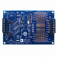
Manufacturer Part Number
EVAL-ADUM540XEBZ
Description
BOARD EVAL FOR ADUM540x
Manufacturer
Analog Devices Inc
Specifications of EVAL-ADUM540XEBZ
Main Purpose
Interface, Digital Isolator
Embedded
No
Utilized Ic / Part
ADuM540x, 520x, 500x, 130x, 131x, 140x, 141x, 240x, 330x, 340x
Primary Attributes
Pads for 16-SOP iCoupler® Isolators, Support for Signal Wrap Back
Secondary Attributes
Places for BNC Connectors for 50 Ohm Signals, Support for isoPower
Lead Free Status / RoHS Status
Lead free / RoHS Compliant


ADuM5401/ADuM5402/ADuM5403/ADuM5404
POWER CONSIDERATIONS
The ADuM5401/ADuM5402/ADuM5403/ADuM5404 power
input, data input channels on the primary side, and data channels
on the secondary side are all protected from premature operation
by UVLO circuitry. Below the minimum operating voltage, the
power converter holds its oscillator inactive and all input channel
drivers and refresh circuits are idle. Outputs remain in a high
impedance state to prevent transmission of undefined states
during power-up and power-down operations.
During application of power to V
is held idle until the UVLO preset voltage is reached. At that
time, the data channels initialize to their default low output
state until they receive data pulses from the secondary side.
When the primary side is above the UVLO threshold, the data
input channels sample their inputs and begin sending encoded
pulses to the inactive secondary output channels. The outputs on
the primary side remain in their default low state because no data
comes from the secondary side inputs until secondary power is
established. The primary side oscillator also begins to operate,
transferring power to the secondary power circuits. The secondary
V
control signal from the secondary is not being generated. The
primary side power oscillator is allowed to free run in this circum-
stance, supplying the maximum amount of power to the secondary,
until the secondary voltage rises to its regulation setpoint. This
creates a large inrush current transient at V
point is reached, the regulation control circuit produces the
regulation control signal that modulates the oscillator on the
primary side. The V
to the load current. The inrush current is less than the short-circuit
current shown in Figure 14. The duration of the inrush depends on
the V
As the secondary side converter begins to accept power from
the primary, the V
side UVLO is reached, the secondary side outputs are initialized to
their default low state until data is received from the corresponding
primary side input. It can take up to 1 μs after the secondary side is
initialized for the state of the output to correlate with the primary
side input.
Secondary side inputs sample their state and transmit it to the
primary side. Outputs are valid about 1 μs after the secondary
side becomes active.
Table 16. Configurations for Power and Data Channels
Power Units
1-Unit Power
2-Unit Power
3-Unit Power
ISO
voltage is below its UVLO limit at this point; the regulation
ISO
loading conditions and the current available at the V
0
ADuM5000 master
ADuM5000 master
ADuM5000 slave
ADuM5000 master
ADuM5000 slave
ADuM5000 slave
ISO
DD1
voltage starts to rise. When the secondary
current is reduced and is then proportional
DD1
, the primary side circuitry
DD1
2
ADuM520x master
ADuM5000 master
ADuM520x slave
ADuM5000 master
ADuM5000 slave
ADuM520x slave
. When the regulation
DD1
pin.
Rev. A | Page 20 of 24
4
ADuM5401 to ADuM5404 master
ADuM5401 to ADuM5404 master
ADuM520x slave
ADuM5401 to ADuM5404 master
ADuM5000 slave
ADuM5000 slave
Number of Data Channels
Because the rate of charge of the secondary side power supply is
dependent on loading conditions, the input voltage, and the output
voltage level selected, take care with the design to allow the
converter sufficient time to stabilize before valid data is required.
When power is removed from V
and coupler shut down when the UVLO level is reached. The
secondary side stops receiving power and starts to discharge. The
outputs on the secondary side hold the last state that they received
from the primary side. Either the UVLO level is reached and
the outputs are placed in their high impedance state, or the
outputs detect a lack of activity from the primary side inputs
and the outputs are set to their default low value before the
secondary power reaches UVLO.
INCREASING AVAILABLE POWER
The ADuM5401/ADuM5402/ADuM5403/ADuM5404 are
designed with the capability of running in combination with
other compatible isoPower devices. The RC
ADuM5401/ADuM5402/ADuM5403/ADuM5404 to provide its
PWM signal to another device acting as a master to regulate its
self and slave devices. Power outputs are combined in parallel
while sharing output power equally.
The ADuM5401/ADuM5402/ADuM5403/ADuM5404 can only
be a master/standalone, and the ADuM5200 can only be a
slave/standalone device. The ADuM5000 can operate as either a
master or slave. This means that the ADuM5000, ADuM520x,
and ADuM540x can only be used in the master slave combinations
listed in Table 15.
Table 15. Allowed Combinations of isoPower Parts
Master
ADuM5000
ADuM520x
ADuM540x
The allowed combinations of master and slave configured parts
listed in Table 15 is sufficient to make any combination of
power and channel count.
Table 16 illustrates how isoPower devices can provide many
combinations of data channel count and multiples of the single
unit power.
ADuM5000
Yes
No
Yes
6
ADuM520x slave
ADuM520x slave
ADuM5000 slave
ADuM5401 to ADuM5404 master
ADuM121x
ADuM5401 to ADuM5404 master
ADuM5401 to ADuM5404 master
DD1
ADuM520x
Yes
No
Yes
, the primary side converter
Slave
OUT
pin allows the
ADuM540x
No
No
No
Related parts for EVAL-ADUM540XEBZ
Image
Part Number
Description
Manufacturer
Datasheet
Request
R

Part Number:
Description:
EVAL BD For QSOP & SOIC16 Dig Isolators
Manufacturer:
Analog Devices Inc
Datasheet:

Part Number:
Description:
IC, ADJ LDO REG, 1.5V TO 5V 250mA MSOP-8
Manufacturer:
Vishay
Datasheet:

Part Number:
Description:
IC, ADJ LDO REG, 1.5V TO 5V 0.6A 8-TSSOP
Manufacturer:
Vishay
Datasheet:
Part Number:
Description:
IC, ADJ LDO REG, 1.5V TO 5V 250mA MSOP-8
Manufacturer:
Vishay
Datasheet:

Part Number:
Description:
IC ADJ LDO REG 1.5V TO 5V 150mA 5-SOT-23
Manufacturer:
Vishay
Datasheet:

Part Number:
Description:
BOARD EVAL AS1324-AD
Manufacturer:
austriamicrosystems
Datasheet:
Part Number:
Description:
IC, ADJ LDO REG, 1.5V TO 5V 0.6A 8-TSSOP
Manufacturer:
Vishay
Datasheet:

Part Number:
Description:
IC, ADJ LDO REG, 1.5V TO 5V, 0.3A, MSOP8
Manufacturer:
Vishay
Datasheet:
Part Number:
Description:
IC, ADJ LDO REG, 1.5V TO 5V, 0.3A, MSOP8
Manufacturer:
Vishay
Datasheet:
Part Number:
Description:
IC, ADJ LDO REG 1.215V TO 5V 0.3A MSOP-8
Manufacturer:
Vishay
Datasheet:

Part Number:
Description:
±1.7g Dual-Axis IMEMS Accelerometer Evaluation Board
Manufacturer:
Analog Devices Inc
Datasheet:

Part Number:
Description:
IC MULTIPLIER ANALOG 8-SOIC T/R
Manufacturer:
Analog Devices Inc
Datasheet:
Part Number:
Description:
IC ANALOG MULTIPLIER 8-DIP
Manufacturer:
Analog Devices Inc
Datasheet:
Part Number:
Description:
IC ANALOG MULTIPLIER 8-SOIC
Manufacturer:
Analog Devices Inc
Datasheet:
Part Number:
Description:
IC ANALOG MULTIPLIER 8-DIP
Manufacturer:
Analog Devices Inc
Datasheet: